FPGA BGA assembly patch manufacturer
Name: FPGA PCB assembly patch manufacturer
Number of SMT lines: 7 high-speed SMT patch supporting production lines
SMT daily production capacity: more than 30 million points
Testing Equipment: X-RAY Tester, First Piece Tester, AOI Automatic Optical Tester, ICT Tester, BGA Rework Station
Placement speed: CHIP component placement speed (at best conditions) 0.036 S/piece
The smallest package that can be attached: 0201, the accuracy can reach ±0.04mm
Minimum device accuracy: PLCC, QFP, BGA, CSP and other devices can be mounted, and the pin spacing can reach ±0.04mm
IC type patch accuracy: it has a high level for mounting ultra-thin PCB boards, flexible PCB boards, gold fingers, etc. Can be mounted/inserted/mixed TFT display driver board, mobile phone motherboard, battery protection circuit and other difficult products
FPGA PCB Board Features
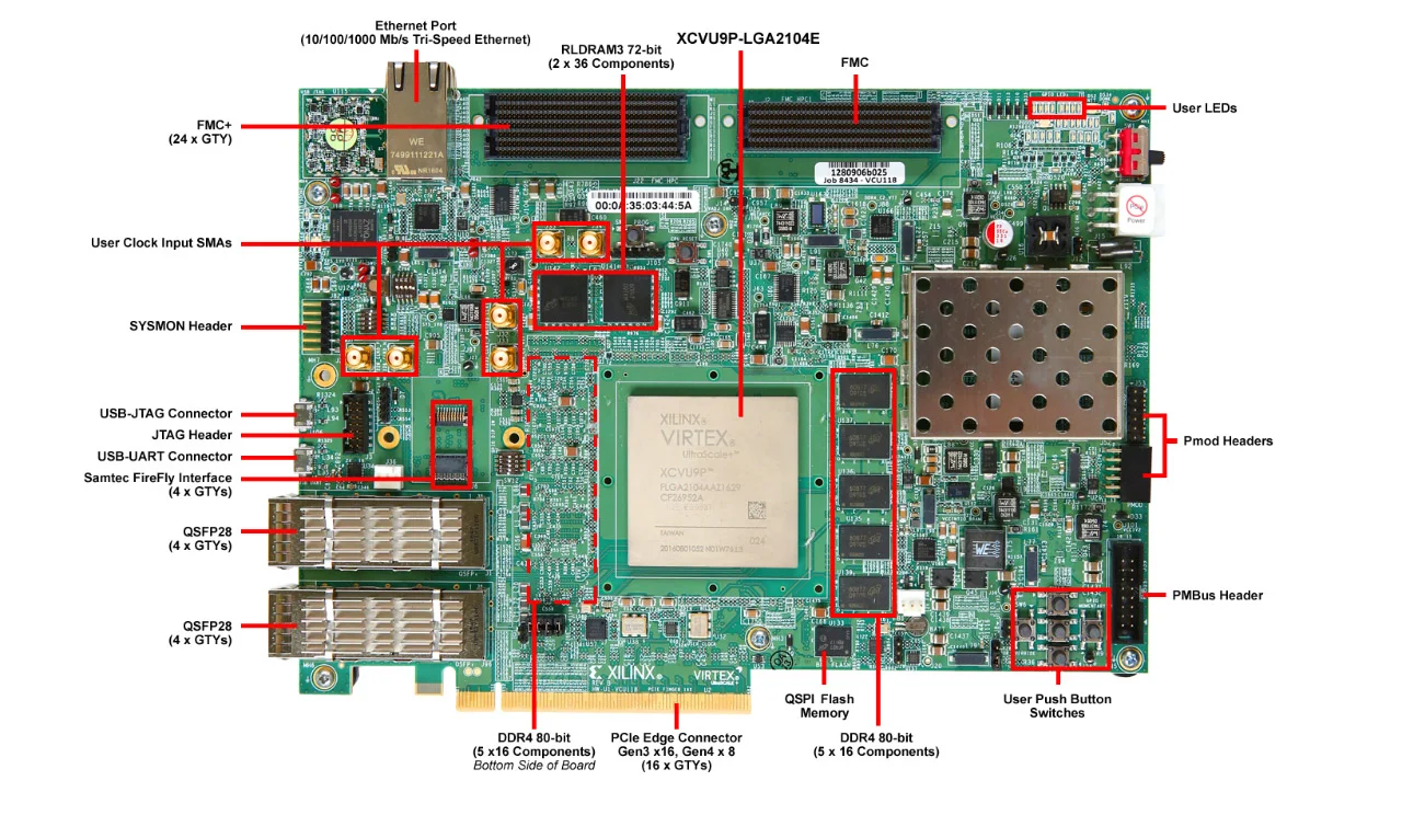
The VCU118 evaluation board features are listed here. Detailed information for each feature is provided in Component Descriptions in Chapter 3.
Virtex UltraScale+ XCVU9P-L2FLGA2104 device
Zynq®-7000 SoC XC7Z010 based system controller
Two 2.5 GB DDR4 80-bit component memory interfaces (five [256 Mb x 16] devices each)
288 MB 72-bit RLD3 memory interface comprised of two 1.125 Gb 36-bit devices
Dual 1 Gb Quad SPI flash memory (BPI flash on pre-Rev. 2.0 boards)
USB JTAG interface using a Digilent module with separate micro-B USB connector
Clock sources:
Si5335A quad clock generator
Three Si570 I2C programmable LVDS clock generators
One SG5032 fixed 250 MHz LVDS clock generator
Si5328B clock multiplier and jitter attenuator for QSFP
Subminiature version A (SMA) connectors (differential)
52 GTY transceivers (13 Quads)
FMC+ HSPC connector (twenty-four GTY transceivers)
2x28 Gb/s QSFP+ connectors (eight GTY transceivers)
Samtec Firefly connector (four GTY transceiver)
PCIe 16-lane edge connector (sixteen GTY transceivers)
PCI Express endpoint connectivity
Gen1 16-lane (x16)
Gen2 16-lane (x16)
Gen3 8-lane (x8) (Pre-Rev. 2.0 VCU118 board VCCINT = 0.72V)
Gen3 16-lane (x16) (VCU118 Rev. 2.0 and later VCCINT = 0.85V
Ethernet PHY SGMII interface with RJ-45 connector
Dual USB-to-UART bridge with micro-B USB connector
I2C bus
Status LEDs
User I/O (4-pole DIP switch, 6 each push-button switches, 8 x LED)
Two Pmod 2x6 connectors (one male pin header, one right-angle receptacle)
VITA 57.4 FMC+ HSPC connector J22
VITA 57.1 FMC HPC1 connector J2
Power management with PMBus voltage monitoring through Maxim power controllers and GUI
10-bit 0.2 MSPS SYSMON analog-to-digital front end
Configuration options:
Dual Quad SPI flash memory
Digilent USB configuration module
Platform cable USB II interface 2x7 2 mm connector

Name: FPGA PCB assembly patch manufacturer
Number of SMT lines: 7 high-speed SMT patch supporting production lines
SMT daily production capacity: more than 30 million points
Testing Equipment: X-RAY Tester, First Piece Tester, AOI Automatic Optical Tester, ICT Tester, BGA Rework Station
Placement speed: CHIP component placement speed (at best conditions) 0.036 S/piece
The smallest package that can be attached: 0201, the accuracy can reach ±0.04mm
Minimum device accuracy: PLCC, QFP, BGA, CSP and other devices can be mounted, and the pin spacing can reach ±0.04mm
IC type patch accuracy: it has a high level for mounting ultra-thin PCB boards, flexible PCB boards, gold fingers, etc. Can be mounted/inserted/mixed TFT display driver board, mobile phone motherboard, battery protection circuit and other difficult products
- Previous:Medical motherboard BGA assembly
- Next:No


