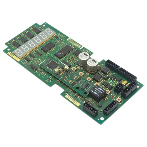
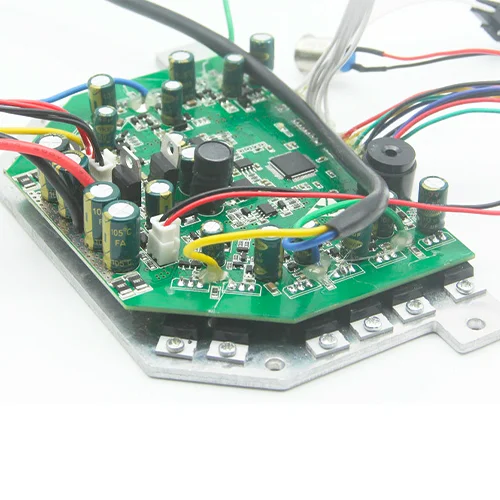
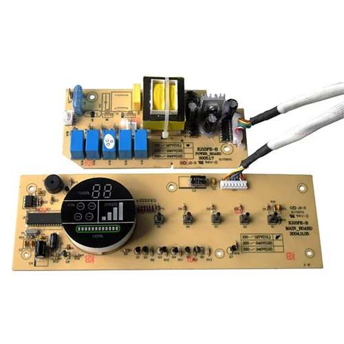
In PCBA processing, with the chip processing equipment more and more powerful, PCB and electronic components are becoming smaller and smaller, SMT chip processing is becoming more and more popular, chip processing gradually replace the previous plug-in processing. But some circuit boards still need plug-in processing, plug-in processing in the current electronic processing industry is still very common, DIP plug-in processing in the SMD processing is completed.
Dual In-line Package, also known as dual in-line package technology, refers to the use of dual in-line package form of integrated circuit chips, the vast majority of small and medium-sized integrated circuits are using this package form, the number of pins generally does not exceed 100
1. BOM checklist, scheduling process
Receive materials according to the BOM bill of materials, check the material type and specification, then arrange the process and assign components for each job
2. Plug-in
Insert the components that need to pass through the hole to the corresponding position of PCBA board, in preparation for wave soldering.
3. Wave soldering machine
Put the plug-in PCBA board into the wave soldering conveyor belt, after spraying flux, preheating, wave soldering, cooling and other links, to complete the wave soldering of PCBA board.
4. Components cutting foot
The finished PCBA board is cut to the right size.
5. Post-soldering
For checking out the finished PCBA board that is not soldered completely should be made up and repaired.
6. Wash the board
Clean the residual flux and other harmful substances on the finished PCBA to achieve the environmental standard cleanliness required by the customer.
7. Testing/quality inspection
After the components are soldered, the finished PCBA products should be tested for functionality, to test whether the functions are normal and to ensure that the products are delivered to customer satisfaction.


