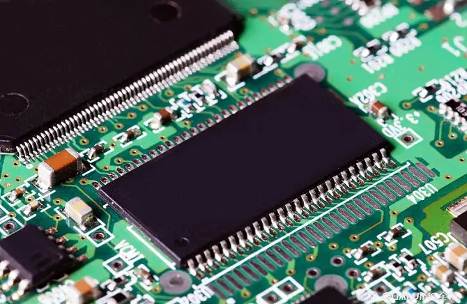
Printed Circuit Board (PCB), Printed Circuit Board (PCB) in Chinese, is one of the important components of the electronic industry. Almost every kind of electronic device, from electronic watches and calculators to computers, communications electronics and military weapon systems, with integrated circuits and other electronic components, uses printed boards for electrical interconnection. In the research process of a larger electronic product, the most fundamental success factors are the design, documentation and manufacture of the printed board for that product. The design and manufacturing quality of printed board directly affect the quality and cost of the whole product, and even lead to the success or failure of business competition.
one Printed circuits provide the following functions in electronic equipment:It provides mechanical support for the fixation and assembly of electronic components such as integrated circuits.

To realize the wiring and electrical connection or electrical insulation between various electronic components such as integrated circuits.Provide the required electrical characteristics, such as characteristic impedance.Provide solder resistance graphics for automatic soldering, identifying characters and graphics for component insertion, inspection and repair.
two Some basic terms for printed boards are as follows:
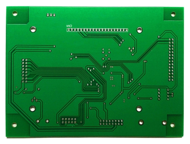
Printed circuit, printed element or conductive pattern formed by combination of the printed circuit, is made on the insulating substrate according to the predetermined design.On the insulating substrate, the conductive pattern that provides the electrical connection between elements and devices is called printed circuit. It does not include printed components.
Printed circuit or finished board of printed circuit is called printed circuit board or printed circuit board, also called printed board.
Printed boards can be divided into two main categories according to whether the substrate used is rigid or flexible: rigid and flexible. Today, there are rigid ----- flexible combination of printed boards. According to the number of layers of the conductor pattern, it can be divided into single-sided, double-sided and multi-layer printed boards.A printed board where the entire outer surface of the conductor pattern is on the same plane as the surface of the substrate is called a flat printed board.
After electronic equipment adopts circait board, due to the consistency of the same type of circait board, so as to avoid the error of manual wiring, and can realize the automatic insertion or placement of electronic components, automatic soldering, automatic detection, to ensure the quality of electronic equipment, improve labor productivity, reduce the cost, and easy to maintain.

Printed boards have evolved from single-layer to double-sided, multilayer, and flexible, and they continue to do so. Due to the continuous development in the direction of high precision, high density and high reliability, and the continuous reduction of size, reduction of cost and improvement of performance, the printed boards still maintain strong vitality in the development of future electronic equipment. 3. Mark of printed board technology level:
The technical level of printed boards is indicated by the number of wires that can be laid between two pads at the intersection of 2.50 or 2.54mm standard grids for double-sided and multi-hole metalized printed boards.
A wire is laid between the two pads, which is a low-density printed board with a wire width greater than 0.3mm. Two wires are arranged between the two pads, which are medium-density printed boards with a wire width of about 0.2mm. Three wires are arranged between the two pads, which are high-density printed boards with a wire width of about 0.10-0.15mm. The ultra-high density printed board can be calculated by laying four wires between two pads, and the line width is 0.05-0.08mm.


