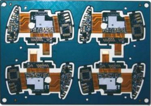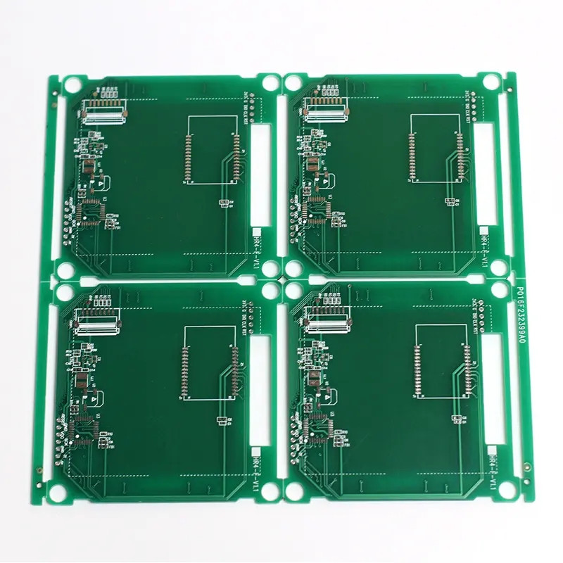
The solder mask of printed circuit board is a permanent protective layer, which not only has the functions of solder protection, protection, improving insulation resistance, but also has a great impact on the appearance quality of the circuit board. In early solder mask printing, PCB solder mask negative was used to make screen graphics, and then UV curable solder mask ink was printed. After each printing, redundant solder mask remains on the bonding pad due to screen deformation, inaccurate positioning and other reasons, which takes a long time to scrape, consuming a lot of manpower and time. Liquid photosensitive solder resist ink does not need to make screen graphics. It adopts empty screen printing and contact exposure. This process has high alignment accuracy, strong adhesion of solder mask, good solderability and high production efficiency, and has gradually replaced light setting ink.
1. PCB process flow
Making solder mask negative → punching negative positioning hole → cleaning printed board → preparing ink → double-sided printing → pre drying → exposure → development → thermosetting
2. Analysis of key process

(1) Prebake
The purpose of pre drying is to evaporate the solvent contained in the ink, so that the PCB solder mask becomes non stick. For different inks, the pre drying temperature and time are different. Too high pre baking temperature or too long drying time will lead to poor development and reduce the resolution; If the pre drying time is too short or the temperature is too low, the negative film will stick when exposed. During development, the solder mask will be eroded by sodium carbonate solution, causing the surface to lose luster or the solder mask to expand and fall off
(2) Exposure
Exposure is the key to the whole process. For positive images, due to light scattering, the solder mask at the edge of the pattern or line reacts with the light (mainly the photosensitive polymer contained in the solder mask reacts with the light) to generate a residual film, which reduces the resolution, resulting in smaller developed patterns and thinner lines; If exposed
If it is insufficient, the result is contrary to the above, and the developed figure becomes larger and the lines become thicker. This situation can be reflected by the test: if the exposure time is long, the measured line width is negative tolerance; If the exposure time is short, the measured line width is a positive tolerance. In the actual PCB process, the "optical energy integrator" can be selected to determine the optimal exposure time.
(3) Ink viscosity adjustment
The viscosity of liquid photosensitive solder resist ink is mainly controlled by the ratio of hardener and main agent and the addition amount of thinner. If the addition of hardener is not enough, it may cause imbalance of ink characteristics. After the hardener is mixed, it will react at room temperature, and its viscosity changes are as follows.
Within 30min: the main ink agent and hardener have not been fully integrated, the fluidity is not enough, and the screen will be blocked during printing.
30min~10h: the main agent of the ink and the hardener have been fully integrated, and the fluidity is appropriate.
After 10h: the reaction between the PCB materials of the ink itself has been actively carried out, resulting in greater fluidity and poor printing. The longer the time after the hardener is mixed, the more fully the reaction between the resin and the hardener is, and then the ink luster becomes better. In order to make the ink glossy and good printability, it is better to place it for 30min after the hardener is mixed.
If the diluent is added too much, it will affect the heat resistance and hardenability of the ink. In short, the viscosity adjustment of liquid photosensitive solder resist ink is very important: viscosity is too thick, screen printing is difficult. The screen plate is easy to stick to the screen; The viscosity is too thin, and the volatile solvent in the ink is more, which brings difficulties to the pre curing.
The viscosity of the ink is measured with a rotary viscometer. In PCB production, the best value of viscosity should be adjusted according to different inks and solvents.


