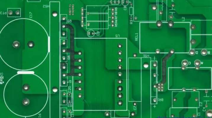
Now many electronics factories only focus on certain aspects, such as marketing, product development and product design. They chose to outsource many aspects of electronics manufacturing. Everyone in the industry knows that a product needs a lot of development and testing time from prototype design to market sale, among which PCBA R&D and proofing is very important. When delivering the designed PCB file and BOM to the PCBA manufacturer, it needs to be analyzed from multiple perspectives to ensure that there is no delay in the project cycle to reduce the risk of product release.

1, market positioning analysis
It is necessary to analyze the market positioning of electronic products to be developed. Different market strategies determine different product development. If it is high-end electronic products, then the sample stand must be strictly selected to ensure that the packaging process, as far as possible to simulate 100% of the real mass production process. If it is a very common electronic product and the solution is mature, concessions can be made at the sample stage, such as using some alternative materials, ICT testing to broaden acceptance, etc.
2, follow the principle of speed over cost
PCBA research and prototyping must follow the principle of speed over cost, from the design out to the PCBA sample back to the hand, usually takes 5 to 15 days. If not well controlled, the time may be extended to 1 month. If the time delay caused by human factors occurs, it will have a great negative impact on the project schedule. In order to ensure that we can receive PCBA samples within 5 days at the earliest, we need to start selecting electronic manufacturing suppliers with manufacturing capabilities, good partnerships, and focus on quality and service at the design stage, even paying 50% of the cost. More proofing charges.
3. Standardize PCB design
The design scheme of the electronic product design company must comply with the specifications as far as possible, such as retaining the cooling hole of the circuit board design, marking the screen printing, conventional treatment of the material in the BOM, and clear marking. This can greatly reduce the communication time with the PCBA processing manufacturer, and also prevent the unclear marking of the design scheme due to production errors.
4, fully consider the risk of logistics distribution link
In PCBA packaging, PCBA manufacturer must provide safe packaging, such as bubble bag, pearl cotton, etc., to prevent collision and damage to the circuit board.
5. PCBA adopts the principle of maximizing the number of research and development samples
The maximization principle should be adopted in determining the number of PCBA samples. General purpose project managers, product managers, general managers, and even marketers may need samples. In addition, the burning plate must be fully considered in the test, so it is usually recommended to make more than 10 samples.
The production of PCBA samples is based on quality and speed. Good communication with PCBA manufacturers is the catalyst. When electronics companies have such a concept, they can gradually form stable partnerships and good design habits, and maximize the smooth progress of the project.
The above is the PCBA research and development proofing for you to share, you need to know what things; There are five things you need to know in total, and those are the ones above. So if you need to carry out PCBA research and development proofing, please contact us electronically. Baiqiancheng Electronics has a professional smt workshop and DIP production line, strength assurance, quality assurance and cost-effective. Experienced maintenance engineers strong maintenance ability, perfect after-sales service; Electronic products patch, welding experience, stable delivery.
Now there are many electronics factories will give their own things to professional processing plants for processing, before mass production is usually carried out PCBA proofing, so what is the PCBA proofing? Customers who need to understand the process of PCBA proofing, together with hundreds of electronic small make up to understand it.
First, customer orders
Customers will according to their actual needs to their own trusted electronic processing plant orders, and put forward specific requirements. The processing plant will evaluate its capacity to see if it can fulfill the order. If the manufacturer is sure that they can complete the order within a certain time, then the two parties will negotiate to determine the production details.
Second, customer data
After the customer decides to place an order, he will provide a series of documents and lists to the electronics processing plant, such as PCB electronic files, coordinate files, BOM list and so on, which must be provided.
Third, purchase raw materials
Electronic processing plant according to the documents provided by the customer to the designated supplier to purchase the relevant raw materials.
Fourth, incoming material inspection
Before PCBA proofing, the electronic processing plant needs to carry out strict quality inspection for all the raw materials to be used, and can only be put into production after ensuring that they are qualified.
Fifth, PCBA production
In the PCBA proofing, in order to ensure the production quality, whether it is patch or welding production, the manufacturer needs to strictly control the furnace temperature.
Sixth, PCBA test
Electronics manufacturers also need to carry out rigorous testing, only passing the test PCB board can be delivered to the customer.
Seventh, packaging after sale
After the PCBA proofing is completed, the product needs to be packaged and then handed over to the customer to complete the whole proofing work.


