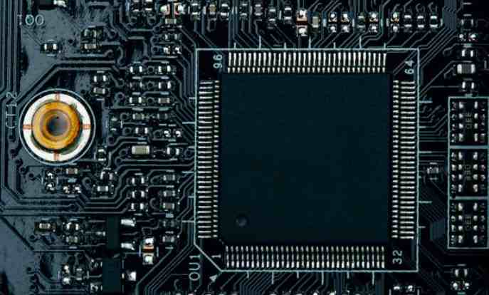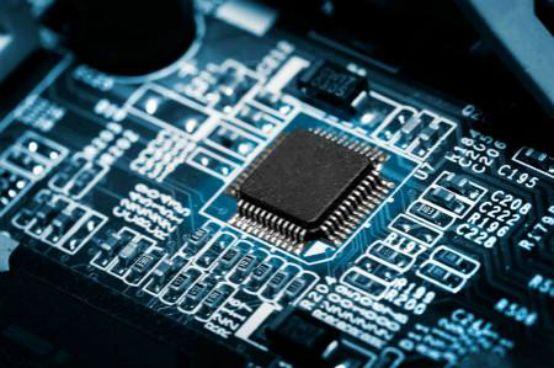
The current circuit board is mainly composed of:
1. Circuit and Pattern: Circuit is used as a tool for conduction between originals. In the design, large copper surface will be designed as the grounding and power layer. The lines and drawings are made at the same time.
2. Dielectric layer: They will be used to maintain insulation between the line and each layer, commonly known as the substrate.
3. Through hole/via: Through hole can make two or more levels of the line through each other, the larger through hole is used as part plug-in, in addition to the non-through hole (nPTH) is usually used as surface mounting positioning, assembly for fixing screws.
4. Solder resistant ink (Solder resistant /Solder Mask) : Not all the copper surface needs to eat the parts on the tin. Therefore, a layer of material (usually epoxy resin) that prevents the copper surface from eating the tin will be printed in the non-solder area to avoid short circuit between the non-solder lines. According to different processes, divided into green oil, red oil, blue oil.
5. Legend /Marking/Silk screen: This is not necessary, and its main function is to mark the name and position frame of each part on the circuit board for convenient maintenance and identification after assembly.
6. Surface Finish: Because the copper surface is easily oxidized in the general environment, it can not be tinned (poor soldering), so it will be protected on the copper surface to eat tin. Protection of the way has TIn spray (HASL), gold (ENIG), Silver (Immersion Silver), tin (Immersion tin), organic flux (OSP), each method has advantages and disadvantages, collectively known as surface treatment.

PCB board characteristics
1. High density: For decades, the high density of printed boards can be developed with the improvement of integrated circuit integration and the advancement of installation technology.
2. High reliability: Through a series of inspections, tests and aging tests, the PCB can be guaranteed to work reliably for a long term (generally 20 years).
3. Designability: For various performance (electrical, physical, chemical, mechanical, etc.) requirements of PCB, printed board design can be realized through design standardization, standardization, etc., with short time and high efficiency.
4. Producability: Adopt modern management, can carry out standardization, scale (quantity), automation and other production, ensure the consistency of product quality.
If the hole breaking state is the phenomenon of dotted distribution rather than the whole circle break, it is called dotted hole breaking, and some people call it "wedge hole breaking". The common cause of this phenomenon is the poor treatment of rubber removal slag. During the processing of PCB circuit board, the slag removal process will first be treated with leavening agent, and then the erosion operation of strong oxidant "permanganate". This process will remove the slag and produce microporous structure. After the removal process of residual oxidizer, rely on reducing agents to remove, typically using acidic liquid treatment.
Because there will be no residual slag problem after slag treatment, we often ignore the monitoring of reducing acid, which may allow the oxidizer to remain on the pore wall. After the circuit board into the chemical copper process, after the whole hole agent treatment of the circuit board will be micro corrosion treatment, then the residual oxidizer is again acid soaked and let the residual oxidizer resin peel off, but also equal to the destruction of the whole hole agent.
The damaged pore wall will not react in the subsequent palladium colloid and chemical copper treatment, and these areas show no copper precipitation phenomenon. The foundation is not established, of course, electroplated copper can not be covered completely and produce punctured holes. This kind of problem has occurred in many circuit board factories in circuit board processing, pay more attention to the removal of glue slag process reduction steps potion monitoring should be able to improve.
Every link in the process of PCB circuit board processing needs our strict control, because chemical reactions sometimes occur slowly in the corners we do not pay attention to, thus destroying the entire circuit. People should be wary of this kind of broken state.
Bare Board (with no parts attached) is also often referred to as the "Printed Wiring Board (PWB)". The substrate of the board itself is made of an insulating, non-bendable material. The small wire material that can be seen on the surface is copper foil. Originally, copper foil is covered on the whole board, but in the manufacturing process, the middle part is etched away, and the remaining part becomes a network of small lines. These lines are called wires or wiring, and are used to provide circuit connections for the components on the PCB board.
Usually the PCB board is green or brown in color, which is the color of solder mask. It is an insulating protective layer, which can protect copper wire, prevent short circuit caused by wave welding, and save the amount of solder. A silk screen is also printed on top of the solder shield. It is usually printed with words and symbols (mostly white) to indicate the position of the parts on the board.


