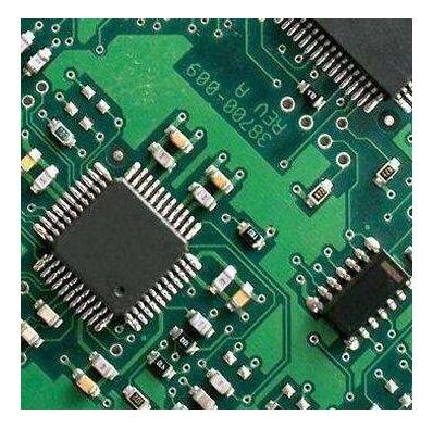
In SMT process, it is easy for the circuit board to warpage when reflow welding. If it is serious, it will even cause bad component welding and tablet erection. How to overcome it? The causes of PCB board warping may be different, but in the end, they can all be attributed to the fact that the stress applied to the PCB board exceeds the stress that the board material can withstand. PCB board warping occurs when the stress on the board is not uniform, or the ability of each part of the board to resist stress is not uniform.
Where does the stress on the board come from? In fact, the biggest source of stress in reflow soldering process is temperature, which will not only make the circuit board soft, but also distort the circuit board, coupled with the coefficient of thermal expansion (CTE) factor and the material characteristics of thermal expansion and cold contraction, which will form the PCB board warping.
As for why some boards warped differently? In my opinion, there are mainly several reasons:
1. The uneven copper surface area on the circuit board will worsen the warpage of the PCB board.

Generally, a large area of copper foil will be designed on the circuit board for grounding, and sometimes Vcc layer will also be designed with a large area of copper foil. When these large areas of copper foil are not evenly distributed on the same circuit board, it will cause the problem of uneven heat absorption and heat dissipation speed. Of course, the circuit board will also expand and shrink. If the expansion and contraction cannot be done at the same time, it will cause deformation under different stresses. At this time, if the temperature of the board has reached the upper limit of Tg value, the board will begin to soften, resulting in permanent deformation.
2. Through holes (vias) in each layer of the circuit board will limit board growth and shrinkage
Most of today's circuit boards are multilayer boards, and there will be rivet holes (via) between the layers, and the holes are divided into through holes, blind holes and buried holes, where the holes will limit the effect of cold expansion and contraction of the board, but also indirectly cause the PCB board warping.
3. The weight of the circuit board itself will cause the board to warp and deform
General reflow furnace will use a chain to drive the circuit board forward, that is, to both sides of the board when the fulcrum to support the whole board, if the circuit board above the excess parts, or the size of the board is too large, it will show the middle sag phenomenon because of its weight, resulting in warping.
4. The depth of V-Cut and the connection strip will affect the deformation of the plate
Basically, V-Cut is the culprit of damaging the structure of the board, because V-Cut is in the original a large sheet of the board to cut out V-shaped grooves, so the V-Cut place is prone to deformation.
In view of the above mentioned problems, in the design and production should pay special attention to the following situations, in order to better avoid the board warping:
1. Reduce the influence of temperature on the stress of the plate
Since the temperature is the main source of the stress of the board, the warping of PCB circuit board can be greatly reduced by reducing the temperature of the backwelding furnace or slowing down the heating and cooling speed of the board in the backwelding furnace. But there may be other side effects, such as a short circuit in the solder.
2. High Tg plate is used
Tg is the glass conversion temperature, that is, the temperature at which the material changes from glass state to rubber state. The lower the Tg value is, the faster the board will become soft after entering the backwelding furnace, and the longer it will take to become soft rubber state, the more serious the deformation of the board will be. The plate with higher Tg can increase its ability to withstand stress and deformation, but the price of the material is relatively high.
3. Increase the thickness of the circuit board
Many electronic products in order to achieve the purpose of thinner, the thickness of the board has been left 1.0mm, 0.8mm, and even 0.6mm thickness, such a thickness to keep the board in the welding furnace without deformation, really a bit of force, it is suggested that if there is no light and thin requirements, the board can use the best thickness of 1.6mm, It can greatly reduce the risk of warping and deformation of PCB board.

4. Reduce the size of the circuit board and reduce the number of boards
Since most backwelding furnaces use chains to drive the circuit board forward, the larger the size of the circuit board will sag and deform in the backwelding furnace because of its own weight, so try to put the long side of the circuit board as the board side on the chain of the backwelding furnace, you can reduce the weight of the circuit board caused by the sag deformation, reduce the number of plates is also based on this reason, That is to say, when the furnace, as far as possible to use the narrow side of the vertical direction of the furnace, can achieve the lowest depression deformation.
5. The tray fixture has been used
If the above methods are difficult to do, the last is to use the furnace tray (reflow carrier/template) to reduce the deformation of the circuit board, the principle that the furnace tray fixture can reduce the warpage of the PCB board is because the fixture material will generally choose aluminum alloy or synthetic stone with high temperature resistance characteristics, Therefore, after the high temperature expansion of the circuit board in the backwelding furnace and the cold contraction after cooling, the tray can play the function of stabilizing the printed circuit board. When the temperature of the circuit board is lower than the Tg value and begins to recover and harden, the original size can still be maintained.
If a single layer of tray fixture can not reduce the deformation of the circuit board, it is necessary to add a layer of cover, the circuit board with two layers of tray clip up, so that you can greatly reduce the circuit board over the welding furnace deformation problem. But the trays are expensive, and you have to add labor to place and retrieve them.
6. Use the Router instead of the V-Cut
Since V-cuts can damage the structural strength of the board, try not to use V-Cut subboards, or reduce the depth of the V-Cut.


