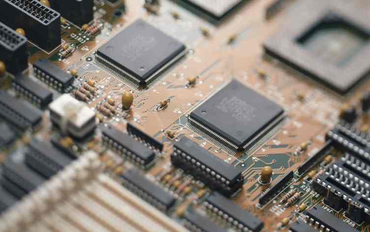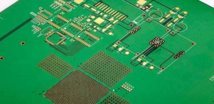
With the development of the electronic industry, the integration degree of electronic components is getting higher and higher, and the volume is getting smaller and smaller, and the BGA type package is widely used. As a result, PCB lines will be smaller and smaller, more and more layers. Reducing line width and line spacing is to maximize the use of limited area, and increasing the number of layers is to use space. The circuit mainstream of future circuit boards will be 2 to 3mil, or smaller.
It is generally believed that every increase or upgrade of the production of circuit boards must be invested once, and the investment capital is large. In other words, high-end circuit boards are produced by high-end equipment. However, not every enterprise can afford large-scale investment, and it takes a lot of time and money to do experiments after investment, collect process data and trial production. Such as according to the existing situation of the enterprise to do trial and trial production, and then according to the actual situation and market conditions to decide whether to invest, it seems to be a better way. This paper describes in detail the limit of the width of fine line which can be produced under the condition of common equipment, and the conditions and methods of fine line production.
The general production process can be divided into cap hole acid etching method and graphic electroplating method, both have advantages and disadvantages. The line obtained by acid etching is very uniform, conducive to impedance control, less environmental pollution, but there is a hole broken will cause scrap; Alkali corrosion production control is easy, but the line is not uniform, the environment pollution is also large.
First of all, the first line production is the dry film, different dry film resolution is different, but generally can show 2mil/2mil line width and line distance after exposure, the resolution of ordinary exposure machine can reach 2mil, generally in this range of line width and line distance will not cause problems. In 4mil/4mil line width line distance or above the developer's nozzle, the relationship between pressure and potion concentration is not very big, in 3mil/3mil line width line distance below, the nozzle is the key to affect the resolution, the general application of fan nozzle, the pressure in 3BAR to develop.
Although the exposure energy has a great impact on the line, most dry films currently used in the market generally have a wide exposure range. It can be distinguished at levels 12-18 (25 exposure scale) or 7-9 (21 exposure scale). Generally speaking, a little lower exposure energy is beneficial to the resolution. However, when the energy is too low, dust and various debris in the air will greatly affect it, and it will cause open circuit (acid corrosion) or short circuit (alkali corrosion) in the later process. Therefore, the actual production should be combined with the cleanliness of the darkroom, so that the minimum line width and line distance of the circuit board can be produced according to the actual situation.
The influence of developing condition on resolution is more obvious when the line is smaller. When the line is above 4.0mil/4.0mil, the influence of developing conditions (speed, potion concentration, pressure, etc.) is not obvious; When the line is 2.0mil/ 2.0mil/ mil, the shape and pressure of the nozzle play a key role in whether the line can be developed normally. At this time, the developing speed may decrease significantly, and the concentration of the solution has an impact on the appearance of the line. The possible reason is that the pressure of the fan nozzle is large. So you can develop; Conical nozzle pressure is small, so it is difficult to develop fine lines. In addition, the direction of the plate has obvious influence on the resolution and the side wall of the dry film.
Different exposure machines have different resolutions. At present, one type of exposure machine is air cooled, surface light source, and the other is water cooled, point light source. The nominal resolution is all 4mil. But experiments have shown that 3.0mil/3.0mil can be achieved without special adjustments or operations; Even 0.2mil/0.2 mil; It is also possible to distinguish 1.5mil/1.5mil when the energy is reduced, but it needs to be done carefully and dust and debris are very important. In addition, there was no significant difference in resolution between Mylar and glass surfaces.
For alkali corrosion, there is always a mushroom effect after electroplating, generally only obvious and not obvious distinction. If the circuit is larger than 4.0mil/4.0mil, the mushroom effect is small.
However, when the line is 2.0mil/2.0mil, the influence is very great. The dry film is very difficult to defilm due to the lead tin spilling during electroplating and forming a mushroom shape. The solution is to; 1. Use pulse plating to make the coating uniform; 2. Use a thick dry film, the general dry film is 35-38 microns, the thick dry film is 50-55 microns, the cost is higher, this dry film in acid corrosion effect is better; 3. Electroplate with low current. But these methods are incomplete. It's really hard to have a very complete approach.
Because of the mushroom effect, thin line film removal is very troublesome. Since the corrosion of sodium hydroxide on lead tin is very obvious at 2.0mil/2.0mil, it can be solved by thickening lead tin and reducing the concentration of sodium hydroxide during electroplating.

In alkali etching, different wire width speed is different, different line shape speed is different, if the circuit board in the production of line thickness is not special requirements, using 0.25oz copper foil thickness of the circuit board production or 0.5oz base copper etching part, plating copper thinner, lead tin thickening, etc. All have the effect of alkali etching fine line, and the nozzle needs to use a fan. Conical nozzles can only do 4.0mil/4.0mil.
In acid etching and alkali etching, the same line width and line shape speed are different, but in general, dry film is easy to break or scratch the mask film and the surface film in the transmission and the previous process, so it is necessary to be careful in production, acid etching its line effect is better than alkali etching, there is no mushroom effect side etching is less than alkali etching, and the effect of fan nozzle is obviously better than conical nozzle. The impedance change of the line after acid etching is less.
In the process of production, the speed and temperature of the film, the cleanliness of the board and the cleanliness of the diazo sheet have a great influence on the qualified rate, especially on the parameters of the acid etching film and the flat surface of the board; For alkali corrosion, the cleanliness of the exposure is important.
Therefore, it is believed that 3.0mil/3.0mil (referring to film line width and spacing) plate can be produced without special adjustment of ordinary equipment; However, the qualification rate is affected by the environment and the proficiency and operation level of the personnel. Alkali etching is suitable for the production of circuit boards below 3.0mil/3.0mil, unless the base copper is small to a certain extent, the fan nozzle effect is significantly better than the cone nozzle.


