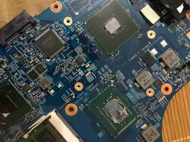
At higher millimeter-wave frequency, the wavelength is short, and the circuit size must be very accurate. The Dk accuracy of dielectric substrate and PCB circuit board materials may directly affect the success of prototype design. The Dk value of the circuit material is determined based on the known physical parameters of the circuit material and the circuit form used in the measurement process and the measurement of the fixture. In fact, there is no perfect measure of Dk. For this reason, there are many different Dk testing techniques that try to achieve the highest accuracy possible. Different methods vary in difficulty and accuracy, and may produce different Dk values even when testing the same material at the same frequency and temperature.
Due to the increasing need for electronic circuits due to millimeter wave applications, uncertainty in Dk values can cause slow design processes. When the Dk of the material is different from the declared value, the Dk value of the circuit sample made from the material must be as accurate as possible to ensure performance, especially the electrical performance of millimeter-wave circuits with fine characteristics. Different Dk testing methods will produce different Dk measurement results, so a basic understanding of the specific differences and significance of Dk testing can be very helpful in millimeter wave circuit design.
As the frequency of circuits and applications increases, a number of different methods have been developed for determining basic parameters such as material Dk and loss factor (Df). All test methods can be roughly divided into two categories: raw material based and circuit based. Raw material-based Dk testing methods tend to place the material into a specific test fixture, whereas circuit-based testing methods make a reference circuit or structure on the material and derive the Dk of the material from the measurement of that circuit or structure. Most raw material-based Dk measurements measure pure dielectric materials with a non-conductive copper foil layer, while circuit-based material measurements include the effect of conductors.
Raw material based Dk testing methods usually measure Dk values at a single frequency and temperature, while circuit-based Dk testing methods can test Dk values at a certain frequency range, depending on the type of test circuit. In addition, circuits based on transmission line structures, such as microstrip lines and strip lines, can be measured in a range of frequencies by continuous sweep measurements, while test circuits using resonators can only test values at a single frequency. Many Dk measurements are standardized according to regulations such as IPC, for example, the IPC TM-650 brings together test methods for determining Dk, loss factor (Df), and other basic material parameters for printed circuit board. However, even with standardization and clear guidelines for the measurement process, different Dk measurements may still yield different Dk values for the same material, simply because of the variables involved in each measurement.
Because different Dk testing methods may produce different Dk values, material vendors provide multiple Dk values for the same material: DKS for process and design. The procedure Dk values here test Dk values at a single frequency and temperature according to the IPC-TM-650 2.5-5.5 standard test method. The design Dk values are a series of values over a range of frequencies. The design Dk value provides the engineer with a more specific Dk value for a material at a certain frequency, especially for the operating frequency of the designed circuit. If there really is no corresponding Dk value, for example at millimeter wave frequencies (30 to 300 GHZ), the designer may have to make his own Dk measurements at the corresponding frequency. Knowing the fact that different Dk test methods produce different Dk values will allow you to better understand the Dk values resulting from your tests when using different Dk measurements.
The accuracy of each Dk test method is affected by a variety of factors, such as the calibration accuracy of the test equipment (such as the vector network analyzer VNA), changes in the fixture used in the raw material-based measurement, or changes in the machining of the transmission line or resonant structure used in the circuit-based Dk measurement. Most circuit materials are anisotropic, that is, Dk values vary along the x (length), y (width), and z (thickness) axes of the material. While the method for determining Dk values on the x and y axes is also useful, the measurement of Dk values on the z axis is usually of the most concern because it represents the Dk values of the transmission line material for most circuits.

The clamp type strip-line resonator test method is the standard test method defined by IPC-TM-650 2.5-5.5 to test the process Dk value and loss factor (Df) of the circuit material. Both parameters are values for measuring material thickness or the z-axis direction. This test method is accurate and repeatable, but only tests Dk values at a single frequency, such as 10GHz. And it represents the characteristics of pure dielectric materials without conductive metal copper foil. To perform this test, the PCB laminate is etched to remove the copper foil, and the measured dielectric material is placed in a fixture containing an internal resonator for measurement. Through the ground floor on both sides of the fixture, a strip line resonance is formed together with the resonator contained in the fixture. In order to make repeated and accurate measurements, the test fixture must be assembled carefully because the air trapped in the fixture containing the material under test (Dk value 1) becomes part of the test and reduces the Dk value of the material determination.
The test fixture is the basic building block of all raw material based Dk test devices. The fixture usually uses some form of resonator to measure physical parameters such as resonant frequency and material thickness so as to determine the Dk value of the material. Thus, the repeatability and accuracy of raw material-based Dk tests depend more on the accuracy of the test fixture, whereas the repeatability and accuracy of circuit-based Dk measurements depend more on the machining impact of the circuit.
Many different types of resonant structures are used to determine Dk values of circuit materials, such as the separated column dielectric resonator (SPDR) method, the full plate resonance (FSR) method, and the separated cylindrical resonator method, which are defined in the IPC-TM-650 measurement method. The SPDR measurement compares an air-filled cavity (cavity) with the same cavity containing the material under test to obtain the Dk value of the material under test. The accuracy of the method depends on the measurement of material thickness and cavity size. What SPDR measures is Dk value in the x-y plane of the material, not Dk value in the z-axis direction. FSR measurements are made using a piece of material with a complete copper foil. The Dk values are obtained by scanning frequency measurements to find the standing wave or resonant peak. A PCB board with a complete copper foil is measured in an operating mode similar to an open parallel plate waveguide, and standing waves along the length of the material board are measured. The material size and resonant frequency can provide sufficient information to deduce the Dk value of the material at this resonant frequency. This method is suitable for applications with long wave length and low frequency, but it is not accurate in measuring thinner materials.
The accuracy of the measurement depends on the precise measurement of the material and the physical dimensions of the circuit, such as the width of the transmission line, the thickness of the copper conductor, and the thickness of the medium. These measurements are more challenging in terms of the size of millimeter-wave circuits and structures. Changes in the thickness of the dielectric material and the roughness of the copper foil conductor may cause changes in the signal path along the transmission line. These changes are more significant at the millimeter-wave frequency and will reduce the Dk measurement accuracy. A smoother copper conductor shortens the signal path along the transmission line and results in different Dk measurements.
In order to determine Dk values of circuit board materials, many test methods have been proposed and validated. The same Dk value can be obtained by using the same test method to test the same sample material at different times. However, different Dk values will be obtained when the same sample is measured using different test methods. The Dk value changes due to the change of test circuit and fixture. This variation can be minimized by using the same test method each time, but the test method may not support providing Dk values at such frequencies as millimeter wave frequencies. With a better understanding of the Dk test method and its variations, it is impossible to find a perfect Dk test, but for relevant applications, at least the best Dk measurement method can be used to determine.


