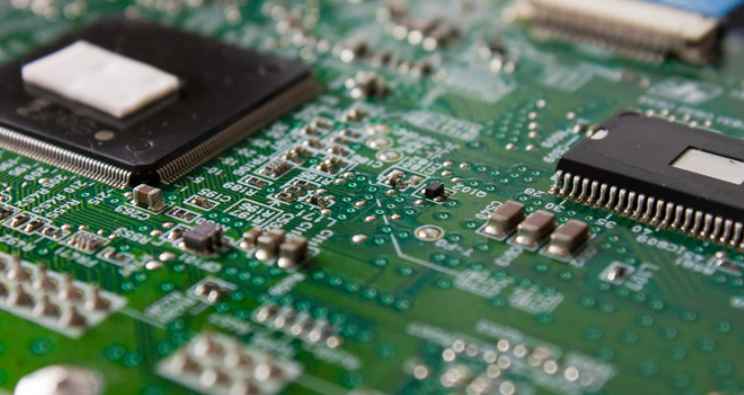
There are usually two ways to solve EMI problems in high-speed PCB (Printed Circuit Board) design: one is to suppress the impact of EMI, the other is to shield the impact of EMI. There are many different manifestations of these two methods, especially the shielding system that minimizes the possibility of EMI affecting electronic products.
Radio frequency (RF) energy is generated by switching currents within printed circuit boards (PCBS) that are a by-product of digital components. Every logical state change in a power distribution system produces a transient surge. In most cases, these logical state changes do not generate enough ground noise voltage to have any functional impact. But when the edge rate (rise time and fall time) of one component becomes quite fast enough radio-frequency energy is generated to affect the normal functioning of other electronic components.
I. Causes of electromagnetic interference on PCB
Improper practices usually cause EMI on PCBS that exceed the specification. Combined with the characteristics of high frequency signal, PCB level EMI mainly includes the following aspects:
(1) Improper use of packaging measures. For example, components that should be encased in metal are encased in plastic.
(2) PCB design is not good, finish quality is not high, cable and connector grounding is not good.
(3) Inappropriate or even wrong PCB layout.
Including improper clock and cycle signal routing setting; Improper arrangement of PCB layer and signal wiring layer; Improper selection of components with high frequency RF energy distribution; Common-mode and differential mode filtering are not considered enough. Ground loop causes RF and ground bomb; Insufficient bypass and decoupling and so on.
To achieve EMI suppression at the system level, some appropriate methods are usually required: this mainly includes shielding, padding, grounding, filtering, decoupling, proper wiring, circuit impedance control, etc.
Second, electromagnetic compatibility shield design
The current electronics industry is increasingly aware of the need for Shielding Effectiveness (SE/EMC) from electronic components, and electromagnetic compatibility is becoming a concern as more electronic components become available. Electromagnetic shielding is the principle of metal isolation to control electromagnetic interference from one area to another area induction and radiation transmission method. Usually includes two kinds: one is electrostatic shielding, mainly used to prevent the influence of electrostatic field and constant magnetic field; The other is electromagnetic shielding, which is mainly used to prevent the influence of alternating electric field, alternating magnetic field and alternating electromagnetic field.
EMI shielding can make the product simply and effectively comply with EMC specifications. When the frequency is below 10MHz, the electromagnetic wave is mostly in the form of conduction, while the electromagnetic wave of higher frequency is mostly in the form of radiation. New materials such as single-layer solid shielding material, multi-layer solid shielding material, double shielding or more than double shielding can be used for EMI shielding design. For low-frequency electromagnetic interference, thick shielding layer is needed. It is most appropriate to use materials with high permeability or magnetic materials, such as nickel-copper alloy, to obtain the maximum electromagnetic absorption loss, while for high-frequency electromagnetic waves, metal shielding materials can be used.

In practical EMI shielding, the electromagnetic shielding efficiency depends largely on the physical structure of the chassis, namely, the continuity of conduction. The seams and openings in the chassis are leakage sources of electromagnetic waves. Moreover, the cables running through the chassis are also the main reason for the decrease in shielding efficiency. The electromagnetic leakage of the opening in the case is related to the shape of the opening, the characteristics of the radiation source and the distance from the radiation source to the opening. The shielding efficiency can be improved by properly designing the size of the opening and the distance from the radiation source to the opening. The usual way to solve the electromagnetic leakage of the shelf gap is to use electromagnetic sealing gaskets at the gap. Electromagnetic sealing gasket is a kind of conductive elastic material, which can maintain the conductive continuity in the gap. Common electromagnetic sealing gaskets are: conductive rubber (conductive particles are mixed into the rubber, so that this composite material has both the elasticity of rubber and the conductivity of metal.) , double conductive rubber (it is not mixed with conductive particles in all parts of the rubber, so as to obtain the benefit of both maximizing the elasticity of the rubber and ensuring electrical conductivity), metal braided mesh sleeve (metal braided mesh sleeve with rubber as the core), spiral tube liner (spiral tube rolled with stainless steel, beryllium copper or tinned beryllium copper), etc. In addition, when the ventilation volume is relatively high, must use the cut-off waveguide ventilation plate, this plate is equivalent to a high pass filter, higher than a certain frequency of electromagnetic wave does not attenuate through, but for the electromagnetic wave below this frequency is greatly attenuated, reasonable application of this characteristic of cut-off waveguide can be very good shielding EMI interference.


