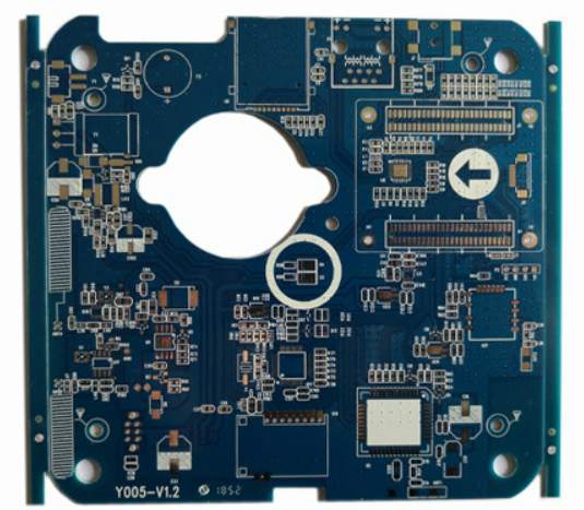
1, poor wetting, leakage welding, virtual welding
Cause:
Welding ends of components, pins, and pads of printed board substrate oxidized or polluted, PCB damp;
Chip components end metal electrode adhesion is poor or the use of single layer electrode, the phenomenon of cap off at welding temperature;
PCB design is not reasonable, the shadow effect caused by wave soldering leakage;
PCB warping, so that PCB warping position and wave soldering contact is bad;
The two sides of the conveyor belt are not parallel (especially when using PCB transmission frame), so that the PCB and the crest contact is not parallel;
The crest is not smooth, the height on both sides of the crest is not parallel, especially the tin wave nozzle of the electromagnetic pump wave welding machine, if blocked by oxide, it will make the crest appear jagged, easy to cause leakage welding, virtual welding;
Poor flux activity, resulting in poor wetting;
PCB preheating temperature is too high, so that the flux carbonization, loss of activity, resulting in poor wetting
The solution:
Components are first come, first use, do not store in a humid environment, do not exceed the specified use date, to clean and dedamp PCB;
The surface mounted components of the three-layer end structure should be selected for wave soldering. The body and welding end of the components can withstand the temperature impact of 260℃ wave soldering more than twice.
When SMD/SMC adopts wave-crest welding, component layout and arrangement direction should follow the principle that smaller components should avoid shielding each other in front and as far as possible. In addition, the length of remaining pad after component lap can be extended appropriately.
PCB warpage is less than 0.8% ~ 1.0%;
Adjust the horizontal level of the crest welder and the transmission belt or PCB transmission frame
Cleaning crest nozzle;
Replace the flux;
Set the appropriate preheating temperature.
2. Pull the tip
Cause:
The preheating temperature of PCB board is too low, so that the temperature of PCB and components is low, and components and PCB absorb heat during welding;
Welding temperature is too low or the speed of the conveyor belt is too fast, so that the viscosity of the molten solder is too large;
The crest height of the electromagnetic pump wave welding machine is too high or the pin is too long, so that the bottom of the pin can not contact the crest, because the electromagnetic pump wave welding machine is hollow wave, hollow wave thickness is 4~5mm
Poor flux activity;
The lead diameter of welding components is not in the correct proportion to the insertion hole. The insertion hole is too large, and the heat absorption of the large pad is large.
The solution:
The preheating temperature is set according to PCB, board layer, the number of components, whether there are attached components, etc. The preheating temperature is 90~130℃;
The temperature of tin wave is (250±5) ℃, and the welding time is 3~5s. When the temperature is slightly low, the speed of conveyor belt should be slowed down.
The crest height is generally controlled at 23 points of the PCB thickness. Pin forming of the plug-in components requires that the pins show the PCB welding surface 0.8~3mm;
Replace the flux;
The aperture of the cartridge hole is 0.15~0.4mm larger than the diameter of the lead (the lower limit is taken for the fine lead and the upper limit is taken for the thick lead).
3, after welding printed board welding resistance film foaming
After welding, SMA will appear light green around individual solder joints. For example, when the ice is high, there will be a bubble the size of a nail, which will not only affect the appearance quality, but also affect the performance. This defect is also a common problem in reflow welding process, but it is common in wave soldering.
Cause:
The fundamental reason for the welding resistance film bubbling is that there is gas or water vapor between the welding resistance film and PCB substrate, these trace gases or water vapor will be included in the different process, when the welding high temperature, gas expansion leads to the welding resistance film and PCB substrate layering, welding, welding temperature is relatively high, so the bubbles first appear around the pad.
Water vapor entrainment in PCB can be caused by one of the following reasons.
PCB in the process of processing often needs to be cleaned and dried before the next process, such as after etching should be dried and then stick welding resistance film, if the drying temperature is not enough, it will entrain water vapor into the next process, in the welding of high temperature and bubbles;
PCB storage environment is not good before processing, the humidity is too high, and the welding is not timely drying treatment;
In wave soldering process, water containing flux is often used now. If the PCB preheating temperature is not enough, the water vapor in the flux will enter the inside of the PCB substrate along the hole wall of the through hole, and the water vapor will enter around the welding pad first. After encountering high welding temperature, bubbles will be produced.
The solution:
Strict control of all production links, purchased PCB should be inspected and stored, usually PCB should not appear bubbling phenomenon within 10 seconds at 260℃;
PCB should be stored in ventilated and dry environment, storage period is not more than 6 months;
PCB should be pre-baked in oven at (120+5) ℃ for 4h before welding;
The preheating temperature in wave crest welding should be strictly controlled. Before entering wave crest welding, it should reach 100~140℃. If the water-containing flux is used, the preheating temperature should reach 110~145℃ to ensure that the water vapor can be volatilized.

4. Pinholes and pores
Pinholes and pores represent that there are bubbles in the solder joint, but they have not expanded to the surface. Most of them occur at the bottom of the substrate. When the bubbles at the bottom are completely diffused and condensed before the explosion, pinholes or pores are formed. The difference between pinholes and pores is that the diameter of pinholes is small.
Cause:
There are organic pollutants on the pins of the substrate or parts. Such contaminated materials come from automatic inserting machines, pin forming machines and poor storage.
The substrate contains water vapor produced by electroplating solutions and similar materials. If the substrate is made of cheaper materials, it is possible to absorb such water vapor and generate enough heat during soldering to vaporize the solution and thus create pores;
The substrate is stored too much or packaged improperly, absorbing water vapor from the nearby environment;
The flux tank contains water;
Excessive moisture in the compressed air for foaming and hot air knives.
The preheating temperature is too low to evaporate water vapor or solvent. Once the substrate enters the tin furnace, it will instantly contact with high temperature and burst.
Tin temperature is too high, in case of moisture or solvent, immediately burst.
The solution:
Remove organic contaminants from pins with common solvent; Due to the difficulty in removing silicone oil and similar silicon-containing products, it is necessary to consider changing the source of lubricating oil or release agent if the problem is found to be caused by silicone oil;
Before assembly, the substrate is baked in the oven to remove the water vapor contained in the substrate;
Bake the substrate in the oven before assembly;
Change flux regularly;
Compressed air needs to be equipped with a water filter, and regular exhaust;
Increase the preheating temperature;
Lower the tin stove temperature.
5. Rough welding
Cause:
Improper time-temperature relationship;
Incorrect solder composition;
Mechanical vibration of solder before cooling;
The tin is contaminated.
The solution:
Adjust conveyor belt speed and correct welding preheating temperature to establish appropriate time-temperature relationship;
Check solder composition to determine solder type and appropriate welding temperature for an alloy;
Check the conveyor belt to ensure that the substrate will not collide or shake during welding and solidification;
Examine the type of impurity causing contamination and reduce or eliminate contaminated solder in the tin tank by appropriate means (dilute or replace solder)
6. Weld into blocks and weld out
Cause:
The conveyor belt speed is too fast;
Welding temperature is too low;
Secondary welding waveform is low;
Improper waveform or waveform and the Angle of the board and the end waveform is improper;
Surface contamination and poor weldability.
The solution:
Slow down the conveyor belt speed; The latest point on it
Adjust the temperature of tin furnace;
Readjust the secondary welding waveform;
Readjust waveform and conveyor belt Angle;
Clean PCB surface and improve its weldability.
7. Too much solder
The welding ends and pins of components are surrounded by excessive solder, and the wetting Angle is greater than 90°.
Cause:
The PCB preheating temperature is too low, and the components and CB absorb heat during welding, which reduces the actual welding temperature.
The activity of flux is poor or the proportion is too small;
Poor weldability of welding pad, cartridge hole or pin, can not be fully infiltrated, resulting in bubbles wrapped in the solder joint;
The proportion of tin in the solder is reduced, or the impurity of Cu in the solder is high, so that the solder viscosity is increased, the fluidity is poor;
Too much solder residue;
Welding temperature is too low or the speed of the conveyor belt is too fast, so that the viscosity of the molten solder is too large.
The solution:
Set preheating temperature according to PCB size, board layer, number of components, whether there are attached components, etc., PCB bottom temperature is 90~130℃;
Change the flux or adjust the appropriate ratio;
Improve the processing quality of the circuit board, components first come first use, do not store in a humid environment;
When the proportion of tin is less than 61.4%, some pure tin impurities can be added properly when the solder should be replaced.
The residue should be cleared at the end of each day;
Control tin wave temperature at (250±5) ℃, welding time 3~5s.
8, tin thin
Causes: poor weldability of component leads, too large pad (except for large pad), too large hole of pad, too large welding Angle, too fast transfer speed, high temperature of tin pot, uneven coating of flux, insufficient tin content of solder.
Solution: To solve the solderability of the lead wire, reduce the welding pad and pad hole during the design, reduce the welding Angle, adjust the transfer speed, adjust the temperature of the tin pot, check the pre-coated flux device, test the solder content.


