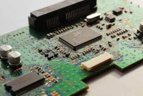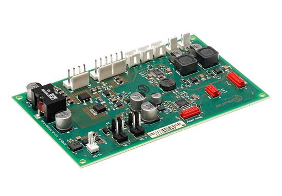
SMT patch proofing is a very important processing link in the process of electronic processing. The precision of SMT patch proofing processing is also very high. Many bad phenomena in electronic processing are some problems in the process of SMT processing. Printing fault is a common adverse phenomenon in the process of patch processing, so most electronic processing plants will try to improve the quality of patch printing, solve and avoid printing fault.
Steel mesh is originally made of wire mesh, so it is called mesh. Nylon (polyester) netting was used at first, and later, because of its durability, barbed wire appeared. Copper wire mesh, and finally stainless steel mesh. But no matter what the material of the screen, there are bad forming screen. The disadvantage of low precision. SMT with the development of the screen board and the requirements of the screen board. Affected by material cost and production difficulty procedures, the original steel mesh was made of iron/copper plates, but due to corrosion, stainless steel mesh replaced them, which is now steel mesh.
The printing method with no gap between the steel mesh and the circuit board is called touch printing. It requires the stability of all structures and is suitable for printing high precision solder paste. The contact between the steel mesh and the circuit board is very smooth and separated from the circuit board after printing. Therefore, the method has a high printing precision, especially suitable for thin spacing and ultra-fine spacing solder paste printing.
Solder paste printing principle: solder paste contact solder paste through the steel plate hole, printed on the substrate tin pad (PCB plate solder plate).
1. Type of scraper: there are plastic scraper and steel scraper, the spacing is not more than 0.5mm IC, steel scraper for printing, easy to print solder paste forming.
2. Adjusting the running viewpoint of the scraper to 45° printing direction can significantly improve the unbalance of different opening directions of the solder paste steel mesh and damage the openings of the fine-spaced steel mesh; The scraper pressure is usually 30N/mm².
3. Printing method: The most common printing methods in SMT processing are "touch printing" and "non-touch printing". The printing method with a gap between the steel mesh and the circuit board is "non-touch printing". Usually the gap value is 0.5~1.0mm, suitable for different viscosity solder paste.
4. Printing speed: Under the push of the scraper, the solder paste will roll on the steel net. SMT patch proofing printing speed is fast, conducive to steel mesh rebound, but also hinder solder paste printing; If the speed is too slow, the solder paste will not roll on the steel mesh, resulting in poor resolution of the solder paste printed on the pad. The printing speed of fine spacing is usually 10~20mm/s.

2. Influence of PCBA small batch proofing and assembly on the overall cost
Printed circuit board, also known as printed circuit board, printed circuit board, often used in English abbreviation PCB, is an important electronic component, is the support body of electronic components, is the circuit connection provider of electronic components. Because it is produced by electronic printing technology, it is called printed circuit board.
In order to understand the high cost of PCBA small batch proofing, we need to decompose the whole process of manufacturing and material contract. PCBA means PCB assembly, which must include circuit board light board, component welding, smt surface mounting and DIP plug-in post welding. The price of light board in the current market is between 350 and 550. The prices of components are basically open and transparent in major shopping malls, which can be compared for reference.
Since the main PCB circuit boards and components are not the possibility of price increases, so the cost is reflected in the link of assembly. The main costs of assembly are as follows:
I. smt patch processing and proofing fee
Patch processing according to the number of points and packaging, there will be a certain difference in price. Large quantity and high price is the consensus of the industry, the larger the component package size, the easier to mount, the corresponding bad quality will be reduced, so the price also has greater room for communication.
2, DIP plug-in after welding hours
Plug-in material link because it involves special-shaped parts and material molding, this link needs a lot of manual participation, because there is no production capacity reference of machinery and equipment, this link is the most difficult to control the cost of the link. At the same time, the labor cost is high, and the cost of this link is generally high.
3, assembly test fee
Test fixture, test equipment, test time, test fixture currently varies from tens to hundreds of yuan according to the difficulty of the test, and the test of communication equipment also needs optical fiber, ICT and other test equipment assistance, the corresponding labor and equipment loss need to be taken into account, but not very high, some companies even test are free.
4, auxiliary costs
The quality of solder paste, solder bar, flux, UV glue, furnace fixture, solder paste and solder bar is the most important auxiliary material in the whole processing liznk, generally domestic solder paste price in 180~260/ bottle, imported solder paste may be in 320~480/ bottle, so the same welding area, the price of imported solder paste is much higher, But the quality of the welds is very different.
kingford one-stop PCBA OEM processing factory, R & D sample/small batch, SMT patch,PCB proofing, DIP welding processing,PCB board, electronic components full purchase, partial purchase one-stop PCBA manufacturing services.


