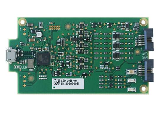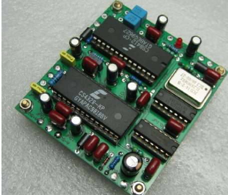
Many friends have questions, why the PCB board color is overwhelmingly green? Next, Shenzhen PCB factory kingford will introduce you.
The PCB board color is mostly green
1, green ink is by far the most widely used, the longest time, but also the cheapest on the market, so green is used by a large number of manufacturers as the main color of PCB products.
2. Under normal circumstances, in the process of making PCB board, several processes must go through the yellow light room, because the effect of green is better than other colors in the yellow light room. In addition, when SMT components are welded, PCB board production needs to go through the solder paste and patch, as well as the final AOI verification process, which requires optical positioning and calibration. The board with green background color has a better recognition effect on the instrument.
3, PCB board production is not necessarily green, depending on the designer wants to make it into what color, it is what color. Common PCB board production colors are red, yellow, green, blue, black. However, due to the production process and other problems, production workers in the case of bright light, naked eyes staring at the board for a long time, easy to cause eye fatigue, relatively speaking, green damage to the eyes is the least.
4. Compared with other colors, the production of green PCB board is very environmentally friendly. When used in high temperature environment, it will not release toxic gases.

2. Use and precautions of reserved process edge in PCB design
The main reason for the reserved process edge in PCB design is that the track of SMT mounter is used to clamp the circuit board and flow through the mounter. Therefore, when components too close to the track edge are absorbed by the suction nozzle of SMT mounter and pasted onto the circuit board, collision will occur and the production cannot be completed. Therefore, in the process of PCB assembling, in order to consider the subsequent patches and plug-ins, Usually you add a craft edge.
Use and precautions of PCB design reserved process edge
The reserved process edge is the part added on both sides or four sides of PCB board to assist the patch plug-in to weld the missing board, which is mainly to assist production and does not belong to the PCB board. It can be removed after the PCBA manufacturing and production is completed.
PCB design reserved process edge will consume more boards, increase the PCB board production cost, so in the design of PCB process edge, need to balance the economy and manufacturability. For some special circuit boards, PCB boards with 2 or 4 process edges can be greatly simplified by means of PCB splicing. SMT processing in the design of the whole way, fully considering the track width, SMT placement machine for more than the width of 350 mm makeup need communication with SMT process engineer of supplier.
PCB design process edge flatness is also an important part of printed circuit board production. When removing PCB design process edges, it is necessary to ensure smooth process edges, especially for circuit boards with high assembly accuracy requirements. Any uneven rough edges will lead to offset installation holes and bring great trouble to subsequent PCBA assembly.
Shenzhen kingford is committed to providing the best and fastest service for the continuous innovation of electronic technology, and becoming the first-class hardware outsourcing service provider in China. The company was founded in 1998, the company headquarters is located in Shenzhen, and Guangdong Shenzhen, Huizhou, Hunan Yiyang established production and operation bases, in Hong Kong branch. For global customers to provide professional PCB design, PCB board, SMT processing, PCBA OEM production (OEM supporting processing), PCB secondary development (can provide chip type identification and chip decryption), radio frequency identification technology (RFID) application, smart card management and development and other quality services.
kingford insists on high quality products, fast delivery time, perfect service, good reputation and flexible marketing as the basis of market competition, and its business has expanded to many countries and regions in Europe, America, Asia and Australia. The future goal is to establish the world's largest manufacturing platform in the sample, small and medium-sized batch field, build the industry's senior technical team, improve the electronic hardware design field technology comprehensive solution ability, combined with supporting multi-variety rapid processing service ability, to provide customers with personalized one-stop service.
kingford actively promotes the one-stop service mode of "PCB design -- manufacturing -- PCBA processing (SMT Mount)" and aims to "create the best overall value for the project", eliminating the inconvenience of multi-party communication, follow-up and coordination of customers in product design, supporting processing and production procurement process management. Through seamless connection of business modules within the company, effectively shorten customer research and development, pilot test and production cycle, reduce the overall cost, and improve the success rate of customer research and development projects through professional technical services. In the field of PCB design, facing the challenges of high speed signal and RF microwave product hardware research and development, the company's technological innovation has always kept pace with the international, providing design for RF communication, PC industrial control, network server, security, digital and other industries customers; At the same time, the SMT processing business of the company is positioned in the mode of rapid delivery of various varieties, providing the whole process services from component purchase, PCB board making, PCBA processing and welding, online testing, complete machine testing, etc., effectively supporting customers to shorten the overall project cycle.


