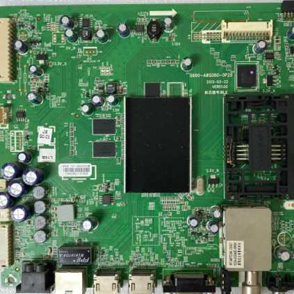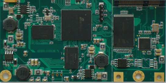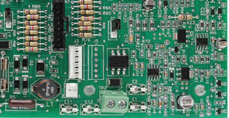
In SMT patch proofing processing, some only need a small number of orders, such as only two or three pieces of sample, in this case there is no need to machine proofing, usually adopt manual SMT proofing processing. SMT patch proofing processing is difficult to paste IC, especially the high integration of IC, the next SMT processing factory in Shenzhen - Shenzhen kingford to introduce SMT patch proofing processing and paste IC matters for attention.
IC is the abbreviation of Integrated Circuit. Industry generally in the form of IC packaging to divide its categories. Traditional ics have SOP, SOJ, QFP, PLCC, etc., while newer ics have BGA, CSP, FLIP CHIP, etc. These part types take on a variety of shapes due to the number and size of pins (part pins) and the spacing between pins. Chip component package form is a semiconductor device package form.
SMT involves a wide variety of parts, different styles, many have formed industry standards, mainly some SMT capacitance resistance; Many are still changing, especially the IC part, the form of packaging changes emerge in endless stream, let a dizzying.
In the processing and production of hand stickers, the difficulty of IC mounting is relatively great, after all, IC is generally a large number of pins, which requires our SMT patch processing personnel to be patient and operate in strict accordance with the processing requirements in order to obtain products with comparable machine stickers quality. For example, due to the high degree of internal integration, easy to be damaged by overheating. Generally speaking, SMT patch proofing processing IC temperature can not be higher than 200℃.

SMT patch proofing processing and installation IC matters needing attention
1. Welding time should be as short as possible, generally no more than 3s.
2, the use of electric iron is the best constant temperature 230 degrees of electric iron.
3, SMT patch proofing table to do anti-static treatment.
4, choose some pointed and narrow iron head, welding will not meet the adjacent endpoint.
5, in the SMT patch processing process, do not remove the pre-set short line before welding CMOS circuit.
6, do not use a knife to scratch the gold-plated circuit pin, just use alcohol or drawing eraser to wipe.
2. Correct method of PCBA processing manual washing plate
After PCBA processing, we often see a lot of residue on the surface of PCBA. These residues not only affect the appearance of PCBA, but most importantly affect the quality of PCBA board. Therefore, PCBA cleaning is very important.
Some small and medium-sized PCBA processing plants usually use the PCBA manual cleaning method, because the manual cleaning method is lower cost and relatively cost-effective. Manual cleaning tools include cleaning cans, spray cans, brushes, IPA or VIGON EFM, gloves, deionized water, wiping paper, air guns, and sealable bags.
PCBA processing manual cleaning steps:
1. Clean the board in IPA or VIGON EFM, or spray IPA and EFM on the board surface, about 10 ml per 4 square inches.
2. Use a wet soft brush to continuously wipe the circuit board for about 10 seconds.
3. Rinse with deionized water, about 10 ml per 4 square inches. Effectively remove potential contaminant residues.
4, handheld circuit board edge, with a clean lint-free wiping cloth to erase excess deionized water.
5. Eye check the cleanliness of the circuit board.
6, if necessary, use air gun to dry the circuit board.
7. If the circuit board or components need to be stored for a period of time before coating, please put the circuit board or components in a sealed bag containing desiccant.
When the batch of PCB circuit boards is relatively large, the disadvantages of manual cleaning will appear, such as the efficiency is relatively low and the washing is not comprehensive and detailed, many electronic components in the gap can not be washed in place, like IC a class of integrated circuit pins a lot, and the substrate is close, brush is not able to enter the inside cleaning. Therefore, PCBA processing manual cleaning plate also gradually began to be replaced by automatic cleaning.
SMT patch processing plant
Shenzhen kingfordSMT processing advantages
1. Strength guarantee
▪SMT workshop: We have imported SMT machines and several sets of optical inspection equipment, with a daily output of 4 million. Each process is equipped with QC personnel, who can keep an eye on product quality.
▪DIP production line: We have two wave-soldering machines, among which there are more than 10 old employees who have worked for more than three years. The skilled workers can weld all kinds of plug-in materials.
2. Quality assurance, cost-effective
▪ High-end equipment can stick precision shaped parts, BGA, QFN, 0201 materials. Can also template patch, loose material hand.
▪ Sample and size batch can be produced, proofing from 800 yuan, batch 0.008 yuan/point, no start-up fee.
3. Rich experience in SMT and welding of electronic products, stable delivery
▪ Accumulated SMT SMT processing services for thousands of electronic enterprises, involving many kinds of automotive equipment and industrial control motherboard. The products are often exported to Europe and the United States, and the quality can be affirmed by new and old customers.
▪ On time delivery, normal 3-5 days after complete materials, small batch can also be expedited on the same day shipment.
4. Strong maintenance ability and perfect after-sales service
▪ Experienced maintenance engineers can repair all kinds of patch welding caused by bad products, to ensure the connection rate of each piece of circuit board.
▪ 24-hour customer service staff at any time response, the fastest speed to solve your order problems.
The above is the introduction of SMT patch proofing processing and installation precautions, if you have PCB products need to do SMT patch proofing, PCBA OEM, welcome to contact Shenzhen Honglijie Electronics!


