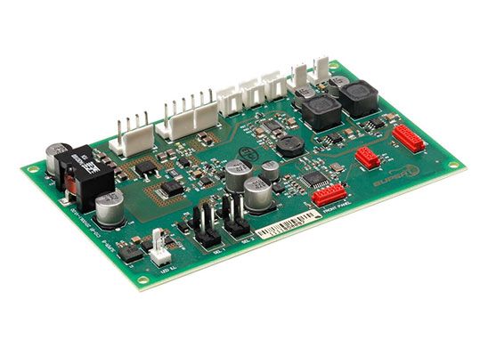
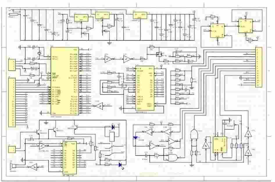
Copper coating as an important part of PCB design, whether domestic PCB design software, or some foreign Protel, PowerPCB provides intelligent copper coating function, so how to apply copper? Next, kingford, Shenzhen PCB design company, will introduce the precautions for copper application in PCB design.
What is copper coating?
The so-called copper coating, is to use the idle space on the PCB board as the base level, and then fill with solid copper, these copper areas are also known as copper filling. The significance of copper coating is to reduce the ground impedance and improve the anti-interference ability; Reduce voltage drop, improve power efficiency; Connected with the ground wire, it can also reduce the area of the loop.
Copper application points for PCB design
1. If the PCB is more, there were SGND, AGND, GND, and so on, is depending on the position of PCB board face, respectively to the main "to" independent copper clad as reference point, to digital and analog to separate apply copper from a few words, at the same time before the copper clad, first bold corresponding power cords: 5.0V, 3.3V and so on. In this way, multiple deformation structures of different shapes are formed.
2. For different single point connections, the practice is through 0 ohm resistance or magnetic beads or inductance connection;
3. The crystal oscillator is coated with copper. The crystal oscillator in the circuit is a high-frequency emission source. The method is to surround the crystal oscillator with copper and then ground the crystal oscillator shell separately.
4. Island (dead zone) problem, if you think it is big, then it is not much of a matter to define a hole to add.
5. At the beginning of wiring, the ground should be equal treatment, when the line should be good ground, can not rely on the copper coating by adding holes to eliminate the pin for the connection, the effect is very bad.
6. It is better not to have a sharp Angle on the PCB board (" =180 degrees "), because from the electromagnetic point of view, this constitutes a transmitting antenna! For other always have an impact on the big or small, I suggest using the edge of the arc.
7. Multilayer intermediate layer wiring open area, do not apply copper. Because it's hard to make the copper "well grounded."
8. The metals inside the device, such as metal radiators and reinforcement bars, must be well grounded.
9. The cooling metal block of the three-end voltage regulator must be well grounded. The grounding isolation belt near the crystal oscillator must be well grounded.
In a word: the copper coating on PCB board, if the grounding problem is handled well, is certainly "more advantages than disadvantages", it can reduce the signal line backflow area, reduce the signal external electromagnetic interference.
2. What are the requirements and specifications for PCB design positioning holes?
In order to facilitate the assembly and processing of the circuit board, the positioning holes will be designed on the PCB board. Next, the requirements and specifications of the positioning holes for PCB design will be introduced.
What are PCB positioning holes?
PCB positioning hole refers to the specific location of PCB hole in the PCB design process, is a very important link in the PCB design process. The function of the positioning hole is the machining benchmark of the printed circuit board. The positioning methods of PCB positioning holes are various, mainly according to the different accuracy requirements. Positioning holes on printed circuit boards should be represented by special graphic symbols. When the requirements are not high, the printed circuit board can also be used in the larger assembly hole instead.
In order to facilitate the PCB drilling and milling of the appearance of the fixed board, as well as the convenience of online testing, many circuit board manufacturers want users to design three nonmetallic holes on the PCB, positioning holes are usually designed to be nonmetallic holes, drilling diameter of mm or. If the Smmo is tight, at least two positioning holes must be placed diagonally. If the board is made, the board can also be regarded as a PCB, the whole board as long as there are three positioning holes. If the user does not place it, the circuit board manufacturer will automatically add it without affecting the circuit, or use the existing nonmetallic holes in the board as positioning holes.
Positioning method of positioning hole
Device Orifice interface devices and connectors are mostly cartridge components. The through hole diameter of the cartridge device is larger than the pin diameter of 8 ~ 20mil, good tin penetration during welding. It should be noted that there is an error in the aperture of the circuit board factory, the approximate error is ±0.05mm, each interval of 0.05mm is a kind of drill, the diameter of 3.20mm above, each interval of 0.lmm is a kind of drill. Therefore, when designing the device aperture, the unit should be converted into millimeters, and the aperture should be designed as an integer multiple of 0.05. The plate manufacturer sets the size of the drilling tool according to the drilling data provided by the user. The size of the drilling tool is usually 0.1 ~ 0.15 larger than the forming hole required by the user. The design aperture should be large rather than small, and the tolerance requirements should also be large rather than small. If it is crimped device, aperture should not increase, according to the data suggested design, and in the board description to explain what is crimped device, so that the circuit board manufacturers can try to control the error in the process of making the board, to avoid some unnecessary trouble.
PCB design positioning hole requirements and specifications
Boreholes are divided into metallized holes and nonmetallic holes. There is copper in the wall of the metallized hole, which can conduct electricity and is represented by PTH. There is no copper in the wall of the nonmetallic hole, so it cannot conduct electricity, which is represented by NPTH. The difference between the outside diameter and the inside diameter of the metallized hole diameter should be greater than 20mil, otherwise the welding ring of the pad is too small for processing and is not conducive to welding. If conditions permit, the aperture can be designed to be the radius of the pad. The maximum bore diameter of metallized hole is 6.35mm, and the maximum bore diameter of nonmetallic hole is 6.5mm. The metallized hole should not be designed on the contour line, and the distance between the edge of the hole and the contour line should generally be greater than 1mm. Heavy cobalt holes tend to damage the bit and should be avoided as much as possible. Non-welding and no electrical characteristics of the hole can be designed into nonmetallic holes, nonmetallic holes do not need to design the welding pad, hole edge distance from the line or copper foil at least 1mmo boreholes can be divided into circular holes and rectangular holes according to the shape, common boreholes are mostly circular holes, rectangular holes are drilled in accordance with the rules of the drill many times, so the rectangular hole design length is twice the width of the best. And the width is not less than 0.8mm, as far as possible to design rectangular holes.
PCB positioning hole requirements:
The development of PCB design industry has tended to mature, so the requirements for PCB positioning holes are also very perfect. The requirements for positioning holes are as follows.
1. At least two positioning holes must be installed on the diagonal of the board.
2, the standard aperture of the positioning hole is 3.2mm _+0.05mm.
3, for different products of the enterprise, the veneer can also use the following preferred aperture: 2.8mm ±0.05mm, 3.0mm±0.5mm, 3.5mm±0.5mm and 4.5mm±05mm. For different boards of the same product (such as DT board and PP board of ZXJlO, etc.), if the PCB outline size is the same, the location of the positioning hole must be the same.
4, the positioning hole is the light hole, that is, the non-metallic through hole (except the radio frequency plate).
5. If the existing mounting holes (except the buckle mounting holes) meet the above requirements, there is no need to set additional bit holes.
Some common specifications and accuracy requirements for positioning holes:
1. The diameter error range of the positioning hole is generally within 0.01mm. A large error in PCB fabrication room will cause poor contact of the probe and incorrect alignment of the automatic mechanism of the interface connector.
2, the diameter of the positioning hole requirements: as far as possible in 3mm below, so that the positioning column will not be deformed, too large is not convenient to operate.
3. Distance of PCB network of positioning hole road: above 1MM, so installation operation is not easy to short circuit, and will not cause damage to the product route.
4, the type of positioning hole: the positioning hole is generally the need for non-sinking copper mechanical control, so that it is not connected with the circuit on the board and higher accuracy.
5. Layout of positioning gallbladder: it needs to be on the four corners or diagonal of PCBA, so as to form multi-point planar positioning, accurate positioning, and the farther away the better.
6, the distance between the positioning hole and the test point should be at least 2mm, to prevent the wrong short circuit in the test.
7. The distance between the positioning hole and the plate edge is at least 2mm, which is not easy to break while ensuring the strength of PCBA.
Shenzhen kingford PCB design capability:
Maximum signal design rate: 10Gbps CML differential signal;
Maximum number of PCB design layers: 40;
Minimum line width: 2.4mil;
Minimum line spacing: 2.4mil;
Minimum BGA PIN spacing: 0.4mm;
Minimum mechanical hole diameter: 6mil;
Minimum laser drilling diameter: 4mil;
Maximum number of pins:; 63000 +
Maximum number of components: 3600;
Maximum number of BGA: 48+.
PCB design service process
1. The customer provides schematic diagram to consult PCB design;
2. Evaluate quotation according to schematic diagram and customer design requirements;
3. The customer confirms the quotation, signs the contract and pays the project deposit;
4. Received advance payment and arranged engineer design;
5. After the design is completed, provide the screenshot of the document to the customer for confirmation;
6. The customer confirmed OK, settled the balance, and provided PCB design materials.


