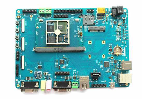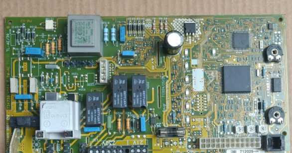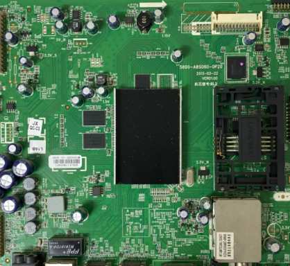
Sometimes there will be some faults after PCBA processing. How to quickly find out the fault point and solve the fault in time is an important part of assessing the technical ability of a PCBA processing plant. Shenzhen kingford has many years of PCBA processing experience, processing of various industries of electronic products, next for you to introduce the rapid repair of PCBA processing after the fault method.
Quick repair of PCBA processing after the fault method
First, visual inspection method
SMT patch faults can be detected by sight, smell, hearing and touch.
Visually check whether there is any error in wiring, solder joints and components of SMT patch, and install the battery after confirming that there is no error. After powering the radio, there is no abnormal sound. If there is no abnormal sound, smell whether there is burnt or not, and touch the transistor with your hand to see whether it is hot and see whether the electrolytic capacitor is cracked.
Two, resistance method
MF47 multimeter is used to test whether the resistance value of the resistance patch components in the circuit is correct, check whether the capacitor is broken, broken or leakage, and check whether the crystal diode and transistor are normal.
Three, voltage method
With MF47 type multimeter DC voltage file test power supply, transistor static working voltage is correct, such as incorrect to find out the reason, but also can detect AC voltage value.
Four, waveform method
Use an oscilloscope to check the circuit waveform, at this time need to be in the case of external signal input, use an oscilloscope to check each transistor output waveform.

5. Current method
Test the collector static current of the transistor with the DC current gear of MF47 multimeter to see if it meets the standard.
Vi. Component substitution method
After the above inspection, if a component is suspected of having problems, it can be replaced by a component with the same specification and in good condition. If the circuit works properly after replacement, it indicates that the original replaced component is damaged. This method is not suitable for components with high cost, because if other components are damaged, unnecessary waste will be caused. For components with high cost, it must be determined that the components are damaged before replacement.
Seven, step by step investigation and separation method
Step by step Check can be performed from the front to the backward or from the back to the forward. Test breakpoints are set between levels so that the detection scope can be narrowed down and the test can be conducted step by step, which makes it easier to locate the fault point.
2. How to remove misprinted solder paste in SMT processing?
How does SMT process remove solder paste misprint? In SMT processing process, misprinted solder paste often occurs. When this happens, some colleagues will use small scraper to remove misprinted solder paste from the board, but using small scraper to remove the solder paste from the misprinted board may cause some problems. Next, we will share with you the effective method of SMT processing to remove misprinted solder paste.
SMT processing to remove misprinted solder paste main methods:
1, will be misprinted board immersed in a compatible solvent, such as adding a certain additive water, washing board water can also be used, and then use a soft brush to remove the small tin beads from the board.
Prefer repeated soaking and washing, rather than violent dry brushing or scraping. After paste printing, the longer the operator waits to clean the misprint, the more difficult it is to remove the paste. Misprinted plates should be placed in a soaking solvent as soon as the problem is discovered, as the solder paste is easily removed before drying.
2. Wash with gentle spray and avoid wiping with cloth strips to prevent solder paste and other pollutants from smeating on the surface of the board. After soaking, it often helps to remove unwanted solder paste.
3. It is also recommended to dry with hot air. If a horizontal template cleaner is used, the face to be cleaned should face down to allow the solder paste to fall off the board.
Attention to a few details can eliminate undesirable situations, such as solder paste misprinting and removal from the plate to solidified solder paste. The goal is to deposit the right amount of paste in the desired location. Soiled tools, dried solder paste, and misalignment of stencil and plate can result in unwanted solder paste on the underside of the stencil or even on the assembly. During the printing process, the stencil is wiped regularly between printing cycles. Ensure that the stencil sits on the pad and not on the solder shield to ensure a clean solder paste printing process. On-line, real-time solder paste inspection and pre-reflow inspection after component placement are all process steps that help reduce process defects before welding occurs.
For fine-pitch formwork, if damage is caused between pins due to the thin stencil cross-section bending, it can cause solder paste to deposit between pins, resulting in printing defects and/or short circuits. Low viscosity solder paste may also cause printing defects. For example, a high press temperature or a high scraper speed can reduce the stickiness of solder paste in use, resulting in printing defects and bridging due to excessive solder paste deposition. In general, lack of adequate material control, solder paste deposition method and equipment are the main reasons for defects in reflow welding process.
There are four reasons to choose kingford for PCBA processing
1. Strength guarantee
▪SMT workshop: We have imported SMT machines and several sets of optical inspection equipment, with a daily output of 4 million. Each process is equipped with QC personnel, who can keep an eye on product quality.
▪DIP production line: We have two wave-soldering machines, among which there are more than 10 old employees who have worked for more than three years. The skilled workers can weld all kinds of plug-in materials.
2. Quality assurance, cost-effective
▪ High-end equipment can stick precision shaped parts, BGA, QFN, 0201 materials. Can also template patch, loose material hand.
▪ Sample and size batch can be produced, proofing from 800 yuan, batch 0.008 yuan/point, no start-up fee.
3. Rich experience in SMT and welding of electronic products, stable delivery
▪ Accumulated SMT SMT processing services for thousands of electronic enterprises, involving many kinds of automotive equipment and industrial control motherboard. The products are often exported to Europe and the United States, and the quality can be affirmed by new and old customers.
▪ On time delivery, normal 3-5 days after complete materials, small batch can also be expedited on the same day shipment.
4. Strong maintenance ability and perfect after-sales service
▪ Experienced maintenance engineers can repair all kinds of patch welding caused by bad products, to ensure the connection rate of each piece of circuit board.
▪ 24-hour customer service staff at any time response, the fastest speed to solve your order problems.


