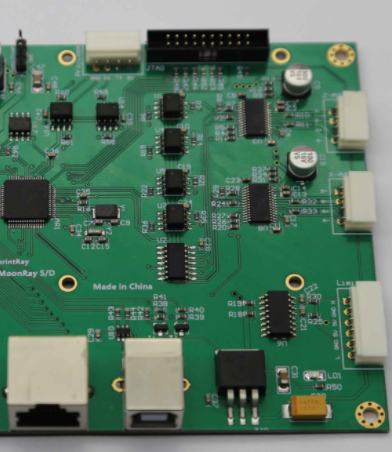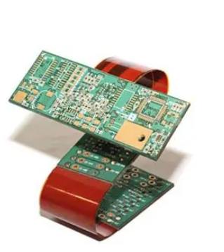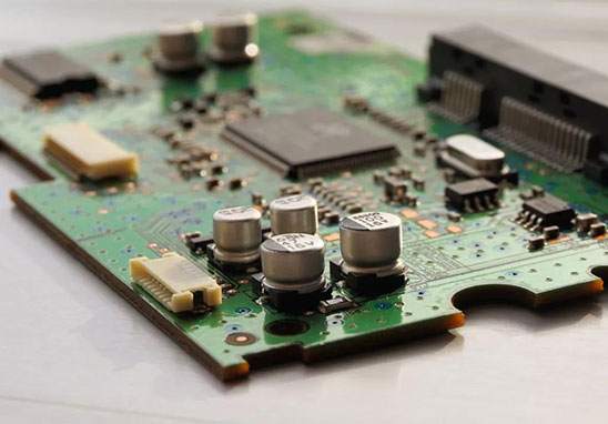
Wiring as the top priority of PCB design process, which will directly affect the performance of PCB board is good or bad, the design process is also the most complicated, higher requirements. Although many advanced EDA tools now provide automatic wiring function, and also quite intelligent, but automatic wiring can not guarantee 100% of the spread rate. Therefore, many engineers are not satisfied with the results of automatic wiring. Manual wiring is still the choice of most engineers, and wiring is restricted by electrical rules to meet the requirements of signal integrity.
After the PCB routing design is complete, check whether the PCB routing design complies with the rules and whether the rules do not meet the requirements of the PCB production process. How to check after PCB wiring? Today brings the PCB wiring inspection method, let's have a look!
General items to be checked after PCB wiring include: General PCB design drawing check items, PCB physical characteristics check items, PCB installation requirements, PCB electrical characteristics check items, PCB mechanical design factors, PCB removal requirements, PCB electrical precautions, PCB mechanical precautions, PCB routing path and positioning, PCB wire spacing, PCB width and thickness, PCB wire graphic check Check the list of items and PCB design items.
1. Check whether the distance between the through holes is reasonable.
2. Check whether the width of the power cable and ground cable is appropriate.
3. Check whether the best measures are taken for key signal cables.
4. Check whether the analog circuit and the digital circuit have independent ground cables.
5. Check whether the graphics added to the PCB cause signal short circuit.
6. Check whether there are process lines on the PCB.
7. Check whether the edge of the outer frame of the power layer on the multi-layer PCB board is narrowed.

There are many points that need to be paid attention to in PCB wiring, and the above inspection items are only a part of them. There will be more problems in the actual work. And the rate of automatic wiring, depends on a good layout, wiring rules including the number of line bending, through the number of holes, the number of steps need to be predetermined in advance. Therefore, if you want to really master PCB wiring, you still need to practice hard, accumulate rich experience, master more rules and skills, in order to gracefully carry out PCB wiring, design a fine and beautiful PCB board.
2. How to avoid PCB warping in SMT processing?
With the miniaturization of electronic devices, the use of thin PCB boards and small components is becoming popular. However, the use of boards with small SMT machining components is not only thin but mostly multilayer PCB, which also presents some problems. Usually, such PCBS warp during smt placement and may eventually affect their production. In addition, excessive warping will also affect the quality of solder paste printing. Warping also affects the formation of solder joints during reflow welding.
What is PCB assembly warping?
SMT process, the circuit board after reflow welding is easy to warping, serious even will cause component welding, tablet and other bad. The causes of PCB board warping may be different, but in the end, they can all be attributed to the fact that the stress applied to the PCB board exceeds the stress that the board material can withstand. PCB board warping occurs when the stress on the board is not uniform, or the ability of each part of the board to resist stress is not uniform.
Where does the stress on the board come from? In fact, the biggest source of stress in reflow soldering process is [temperature], temperature will not only make the circuit board soft, but also distort the circuit board, coupled with the coefficient of thermal expansion (CTE) factor and [thermal expansion and cold contraction] material characteristics, this will form the PCB board warping.
Cause of PCB warping in SMT processing
Internal stresses on the copper film can cause the circuit board to warp. This is possible even at room temperature without any heat treatment.
In processes involving temperature variations, such as reflow welding, warping can occur due to the different coefficient of thermal expansion between the copper layer and the substrate.
When individually etched copper-covered sheets are stacked on top of each other, differences in the density of the copper in each layer can cause different amounts of stress on each layer, resulting in warping.
PCBS are usually placed in panels to improve PCB assembly efficiency. Panels, in turn, use guides and legs. After assembly, the legs are removed and the PCB is separated by disassembly. The difference in copper density between the board area and the outstretched bracket area further causes warping.
SMT machining methods to avoid PCB warping
1. Reduce the influence of temperature on the stress of the plate
Since [temperature] is the main source of stress on the board, the warping of PCB board can be greatly reduced by reducing the temperature of the backwelding furnace or slowing down the heating and cooling speed of the board in the backwelding furnace. But there may be other side effects, such as a short circuit in the solder.
2. High Tg plate is used
Tg is the glass conversion temperature, that is, the temperature at which the material changes from glass state to rubber state. The lower the Tg value is, the faster the board will become soft after entering the backwelding furnace, and the longer it will take to become soft rubber state, the more serious the deformation of the board will be. The plate with higher Tg can increase its ability to withstand stress and deformation, but the price of the material is relatively high.
3. Increase the thickness of the circuit board
Many electronic products in order to achieve the purpose of thinner, the thickness of the board has been left 1.0mm, 0.8mm, and even 0.6mm thickness, such a thickness to keep the board in the welding furnace without deformation, really a bit of force, it is suggested that if there is no light and thin requirements, the board can use the best thickness of 1.6mm, It can greatly reduce the risk of warping and deformation of PCB board.
4. Reduce the size of the circuit board and reduce the number of boards
Since most backwelding furnaces use chains to drive the circuit board forward, the larger the size of the circuit board will sag and deform in the backwelding furnace because of its own weight, so try to put the long side of the circuit board as the board side on the chain of the backwelding furnace, you can reduce the weight of the circuit board caused by the sag deformation, reduce the number of plates is also based on this reason, That is to say, when the furnace, as far as possible to use the narrow side of the vertical direction of the furnace, can achieve the lowest depression deformation.
5. The tray fixture has been used
If the above methods are difficult to do, the last is to use the furnace tray (reflow carrier/template) to reduce the deformation of the circuit board, the principle that the furnace tray fixture can reduce the warpage of the PCB board is because the fixture material will generally choose aluminum alloy or synthetic stone with high temperature resistance characteristics, Therefore, after the high-temperature expansion of the circuit board in the backwelding furnace and the cold contraction after cooling, the tray can play the function of stabilizing the circuit board. When the temperature of the circuit board is lower than the Tg value and begins to recover and harden, the original size can still be maintained.
If a single layer of tray fixture can not reduce the deformation of the circuit board, it is necessary to add a layer of cover, the circuit board with two layers of tray clip up, so that you can greatly reduce the circuit board over the welding furnace deformation problem. But the trays are expensive, and you have to add labor to place and retrieve them.
6. Use the Router instead of the V-Cut
Since V-cuts can damage the structural strength of the board, try not to use V-Cut subboards, or reduce the depth of the V-Cut.


