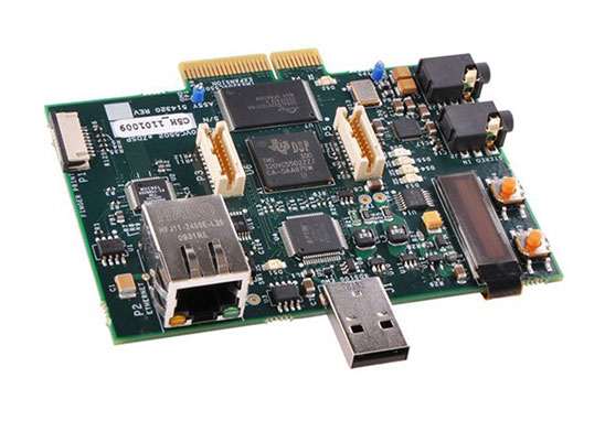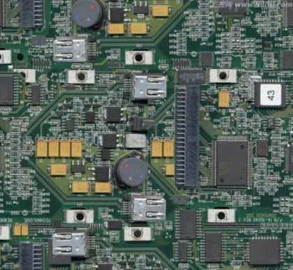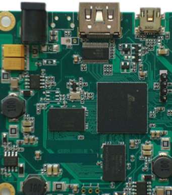
Many newcomers to the industry have doubts about the color of PCB board, do not know what color PCB board is high quality. In fact, PCB mainly provides interconnection between components, its color and performance, quality has no direct relationship, the difference of color will not affect the electrical property. Next, Shenzhen kingford, a PCB manufacturer in Shenzhen, will introduce why PCB board quality has nothing to do with PCB color
The quality of PCB board and PCB color relationship
The raw materials of PCB are found everywhere in our daily life, that is, glass fiber and resin. Glass fiber combined with resin, hardening, into a heat insulation, insulation, and not easy to bend the board, this is PCB substrate. Of course, the PCB substrate made of glass fiber and resin alone cannot transmit signals, so on the PCB substrate, the manufacturer will cover the surface with a layer of copper, so the PCB substrate can also be called copper coated substrate.
There is a situation easy to let people mistakenly think that the quality of PCB board and PCB color is related: individual PCB design using black, in the process of washing PCB, easy to cause color difference; If there is a slight deviation in the raw materials and manufacturing process used by PCB factories, the defective rate of PCB will increase due to the color difference, which directly leads to the increase in production cost. Because the circuit routing of black PCB is difficult to identify, it will increase the difficulty of research and development and after-sales maintenance and debugging. Generally, brands without profound RD(research and development) design personnel and strong maintenance team will not easily use black PCB. Based on the above reasons, most of the major manufacturers use red PCB, green PCB or blue PCB when choosing PCB design for their products, while black PCB is rarely seen.
In short, the performance of PCB board is determined by the material used (high Q value), wiring design and several layers of board and other factors; The quality of PCB board has nothing to do with PCB color.
2. Factors affecting the cost during SMT patch processing
kingford has its own SMT plant, which can provide SMT SMT processing services of 0201 components with minimum package, support incoming material and sample processing and PCBA OEM and materials processing. Next, we will introduce the factors that affect the cost of SMT patch processing.
Advantages of SMT processing
SMT processing from its essence, is through the relevant machinery and equipment to the components of the intact welding to the PCB light board technology. Although the expenditure on the machine cost is relatively large, compared with the traditional plug-in assembly, it has its own unique advantages and characteristics. This technology has many advantages, such as the overall PCBA processing efficiency, miniaturization of components and miniaturization of the finished product volume. Because the machine can produce in large quantities, it greatly improves the cost increase and low efficiency caused by labor-related restrictions, which is the technological upgrade of the development of the entire electronic manufacturing industry.

SMT patch processing involves the main stages
1. Solder paste printing
2. Check the welding paste
3. Patch processing
4, manual inspection
5. Reflow welding
6, in (offline) AOI test
7. X-RAY detection
8. Functional testing
Factors affecting the cost in SMT patch processing
1. Solder paste printing
The process involves placing the exact amount of solder paste on the pad of the component to be welded. For this reason, it is not only important that the solder paste is applied properly, but also that it is stored properly at low temperatures and returned to room temperature before application. In addition, also need to pay attention to the scraping Angle and speed.
2. Check the solder paste
This step goes a long way in reducing costs, as it facilitates early detection of SMT welding defects. What it enables you to do is prevent costly defects in the later stages of manufacturing.
3. Patch processing
An important part of the SMT assembly process, this is done through the SMT mounter. While small components are mounted via high-speed mounters, larger components require multifunctional mounters that operate at low speeds.
4. Manual visual inspection
The visual inspection process again ensures that any defects can be detected early. Some errors that can be identified at this stage include any missing parts or lack of proper placement. After reflow welding, it will be difficult to deal with these defects. Again, this stage of SMT assembly allows cost control as if this stage were not performed, and you can expect to correct errors later and production costs to rise.
5. Reflow welding
This process involves melting the solder paste so that the components can be connected to the circuit board. The temperature curve setting determines reflow welding capability and reduces production costs. Professional fitters can control costs to a large extent.
6. Automatic optical detection
At this stage, the performance of the solder joint is thoroughly checked. Some errors that can be detected at this stage include:
Stele, less, dislocation, bridge, welding and so on.
7. X-ray detection
Once again, X-ray testing is a good way to ensure that the product is efficient and does not have to contend with product defects once the product is released to the market.
8. ICT or functional testing
Functional testing also continues to test the functionality of the assembled PCB to ensure that the final product is very reliable.
PCB board making ability
Energy production from 2 layers to 14 layers, 14-22 layers can be proofing production.
Minimum line width/spacing: 3mil/3milBGA Spacing :0.20MM
Minimum aperture: 0.1mm Size :610mmX1200mm
Ink: Tamura, Taiyo, Fudoken;
FR4: Shengyi, Kingboard, Harbour, Hongren, Guoji, Hezheng, Nanya,
(Shengyi S1130/S1141/S1170),Tg130℃/ Tg170℃ T g180℃ and other high TG plates)
High frequency plate: Rogers, Taconic, ARLLON;
Surface process: tin spray, lead-free tin spray, gold plating, full plate gold plating, plug gold plating, full plate thick gold, chemical tin (silver), anti-oxidation (OSP) blue glue, carbon oil
PCBA proofing process
1. Customers place orders
Customers place orders according to their actual needs of PCBA processing plants, and put forward specific requirements. The processing plant will evaluate its capacity to see if it can fulfill the order. If the manufacturer is sure that they can complete the order within the expected time, then the two parties will negotiate to determine the production details.
2. Production materials provided by customers
After the customer decides to place an order, he shall provide a series of documents and lists to the PCBA processing plant, such as PCB electronic files, coordinate files, BOM list and so on, which must be provided.
3. Purchase raw materials
PCBA processing plant purchases relevant raw materials from designated suppliers according to the documents provided by customers.
4. Incoming material inspection
Before PCBA processing, strict quality inspection is carried out for all raw materials to be used to ensure that they are qualified before being put into production.
5. PCBA production
In the process of PCBA processing, in order to ensure the quality of production, whether it is patch or welding production, the manufacturer needs to strictly control the furnace temperature.
6. PCBA test
The PCBA processing plant conducts rigorous product testing, and the PCB board that passes the test is delivered to the customer.
7. Packaging after sale
After the PCBA processing is completed, the products are packaged and then handed over to the customer to complete the whole PCBA processing.


