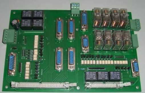
Design of PCB anti-jamming technology
1 Introduction
Electromagnetic Compatibility EMC is the ability of an electronic system to function as designed in a specified electromagnetic environment. The electromagnetic interference of electronic system comes not only from the radiation of electric and magnetic fields, but also from the common impedance of the line, the junction between conductors and the circuit structure. In developing and designing circuits, we also want to design printed circuit boards that are as resistant to external interference as possible, and which themselves interfere with other electronic systems as little as possible. There are many factors affecting the anti-interference performance of printed boards, among which the main factors are the thickness of copper foil, the width and length of printed wire and the crosstalk between adjacent wires, the rationality of the layout of components in the board, the common impedance of wires, the electromagnetic field generated by wires and components in space, etc.
The primary task of designing the printed board is to analyze the circuit and determine the key circuit. This is to identify which circuit is the source of interference, which circuit is sensitive circuit, understand the source of interference through what path interference sensitive circuit. In analog circuits, low-level analog circuits are often sensitive circuits, and power amplifiers are often interference sources. When the working frequency is low, the interference source mainly interferes with the sensitive circuit through the interline barrel closing; When the working frequency is higher, the interference source mainly interferes with the sensitive circuit through electromagnetic radiation. In digital circuits, high speed repeat signals.
Such as clock signal, bus signal contains rich frequency components, is the largest source of interference, often pose a threat to sensitive circuits. Reset circuit, interrupt circuit is sensitive circuit, easy to peak signal interference, then digital circuit can not work normally. The input/output circuit (1/0) is connected to the outside world, and special attention should be paid to it. If the UO circuit is close to the clock line and other interference sources, the unwanted high-frequency energy will be connected to the input and output wires, and the noise on the wires will interfere with the sensitive circuit near the cable through radiation or conduction.

On the basis of the full analysis of the circuit and the determination of the key circuit, the circuit must be properly arranged on the printed board. Such as for digital circuits, should be the high speed circuit (such as clock circuit, high speed logic circuit, etc.), low speed logic circuit and UO circuit layout in different areas, as far as possible in space to separate the interference source and sensitive circuit, so that the interference source of sensitive circuit radiation interference greatly reduced.
2. Anti-interference design of printed board
The purpose of anti-interference design of PCB board is to reduce the electromagnetic radiation of PCB board and the crosstalk between the circuit on PCB board. In addition, PCB ground design also directly affects the common-mode voltage radiation of 1/0 cable. Therefore, the anti-interference design of PCB is of great significance to reduce the electromagnetic information radiation of the system.
2.1 PCB layout design
The density of printed circuit board (PCB) is getting higher and higher, and the quality of PCB design has a great influence on the ability to resist interference, so the layout of PCB is in a very important position in the design.
Layout requirements of special components:
1. The shorter the connection between high-frequency components, the better to minimize the electromagnetic interference between each other; Components susceptible to interference should not be too close to each other; Input and output components should be as far away as possible;
2, some components have a higher potential difference, should increase the distance between them, reduce the common mode radiation. The layout of components with high voltage should pay special attention to the rationality of the layout;
3, the thermal sensitive element should be far away from the heating element;
4. The disconnecting capacitor should be close to the power pin of the chip;
5, for the potentiometer, adjustable inductance coil, variable capacitor, micro switch and other adjustable components layout should be placed in a position convenient to adjust according to the requirements;
6. The position occupied by the printing board positioning hole and the fixing bracket should be set aside.
Layout requirements of common components:
1. Place the devices of each functional circuit unit according to the circuit flow, so that the signal flow direction is as consistent as possible;
2, the core components of each functional circuit as the center, around it to layout, components should be evenly and neatly arranged on the PCB, as far as possible to reduce and shorten the lead and connection between the components;
3. The circuit working at high frequency should consider the interference between components. The general circuit should make parallel arrangement of components as far as possible to facilitate wiring;
4, PCB outplace a line from the edge of the circuit board is generally not less than 80mil. The best shape for a circuit board is a rectangle. The aspect ratio is 3:2 or 4:30.


