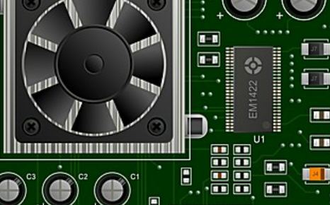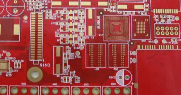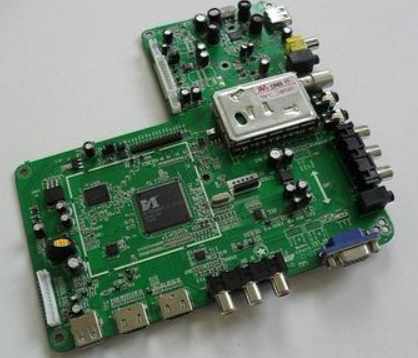
When designing printed plates, attention should be paid to:
The interlayer semi-cured sheet should be arranged symmetrically, such as the thickness of six layers of sheet, 1~2, 5~6 layers of sheet and the number of sheets of semi-cured sheet should be consistent, otherwise it is easy to stratify and warped.
Multilayer core plates and semi-cured sheets shall be manufactured by the same supplier.
The linear areas of the two outer planes A and B should be as close as possible. If side A is large copper and side B only runs a few lines, this type of plate warps easily after etching. If the line area difference between the two sides is too large, several independent grids can be added on the thin side to achieve balance.
3. Welding resistance, character baking and other processes:
Because the solder resistance inks cannot be superimposed on each other when curing, the circuit boards are placed vertically on the shelf for drying boardcuring. The solder resistance temperature is about 150℃, which is just above the Tg point of Tg material. The resin above the Tg point is in high elastic state, and the boards are easy to deform under the action of dead weight or strong wind of oven.
4. Flatness of hot air solder:
The temperature of the tin furnace of the general plate hot air solder machine is between 225℃ and 265℃, and the time is 3S-6S. The hot air temperature is between 280 and 300 degrees Celsius.
Under normal temperature, solder from normal temperature to tin furnace, after two minutes out of the oven, then wash under normal temperature after treatment. The whole process of hot air solder leveling is a rapid cooling process.
Because of the different materials of the circuit board, its structure is not uniform, in the process of heating and cooling will inevitably produce thermal stress, resulting in microscopic strain and overall deformation warped zone.
Step 5 Store:
The printed circuit board is stored in the semi-finished product stage, which is generally hard inserted on the shelf. The shelf tightness is not properly adjusted, or the stacking and placing of the board in the storage process will cause mechanical deformation of the board. In particular, the impact on the plate below 2.0mm is greater.

In addition to the above factors, there are many factors affecting the deformation of PCB board.
Prevent circuit board warping deformation.
The warping deformation of PCB has a great influence on the production of printed circuit boards. Warping deformation is also an important problem in the production of printed circuit boards. The boards installed with components will bend after welding, which makes the feet of components not easy to be neat.
The board cannot be installed in the case or socket, so the warping of the board will affect the overall operation.
At present, the printed circuit board has entered the stage of surface installation and chip installation, and the process requirements are increasing, so the warping requirements of the circuit board are becoming higher and higher. Therefore, we have to find out the cause of the half bend.
According to the type of PCB board reinforcement material, it is usually divided into the following categories:
First, phenolic PCB board.
Because this kind of PCB is composed of paper pulp and wood pulp, so sometimes also become board, V0 board, flame retardant board and 94HB, etc., its main material is wood pulp fiber paper, after the phenolic resin pressurized PCB board.
This kind of cardboard has the characteristics of no fire resistance, punching processing, low cost, low price, low density. We often see phenolic paper substrates are XPC,FR-1,FR-2,FE-3, etc. And 94V0 belongs to the flame retardant board, can be fireproof.
The second is the composite PCB substrate.
These materials are also made into powder boards, reinforced with wood pulp paper or cotton pulp paper, and surface reinforced with fiberglass cloth, both of which are made from flame retardant epoxy resins. Among them, there are single-side semi-glass fiber 22F, CIM-1, two-side semi-glass fiber board CIM-3, among which CIM-1 and CIM-3 are the most commonly used composite base coppers.
Three, glass fiber PCB substrate.
Sometimes also become epoxy board, glass fiber board, FR4, fiberboard, etc., it is made of epoxy resin as adhesive, and reinforced with glass fiber cloth. This kind of board work temperature is higher, the environment is suitable.
Final aperture error:
Unsaturated fatty acid content:
Finished hole wall copper thickness: 18-25um(0.71-0.99mm)
Minimum SMT patch spacing:
Surface coating: chemical precipitator, tinning agent, whole plate nickel plating (water/soft gold), screen printing glue, etc.
Welding resistance layer thickness: 10-30μ
Stripping resistance:
Hardness of welding resistance film: > 5H.
Weld resistance: 0.3-0.8mm
Media constant: ε=2.1-10.0.
· Insulation resistance: 10KΩ-20MΩ.
Characteristic impedance: 60ohm±
Temperature impact: Temperature 288 ° C, temperature 10 ° C.
Warping of finished plate:
· Product Usage: communication equipment, automotive electronics, instruments, GPS, computer, MP4, power supply, household appliances, etc.


