Electromagnetic compatibility refers to the ability of electronic devices to work harmoniously and efficiently in various electromagnetic environments. The purpose of EMC design is to enable electronic equipment not only to suppress all kinds of external interference, so that electronic equipment can work properly in a specific electromagnetic environment, but also to reduce the electromagnetic interference of electronic equipment itself to other electronic equipment.
Follow the following PCB design tips to effectively improve the electromagnetic compatibility of the board:
First, choose a reasonable wire width
The inductance of the printed wire should be reduced as much as possible because the impulse interference of the transient current on the printed wire is mainly caused by the inductance component of the printed wire. The inductance of printed wire is proportional to its length and inversely proportional to its width, so a short and fine wire is advantageous to restrain interference. The signal lines of clock leads, line drivers, or bus drivers often carry large transient currents, and printed wires should be kept as short as possible. For discrete component circuit, printed wire width in about 1.5mm, you can fully meet the requirements; For integrated circuits, the printed wire width can be selected between 0.2 and 1.0mm.
Two, the use of correct wiring strategy
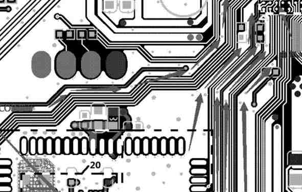
The use of equal wiring can reduce the inductance of the wire, but the mutual inductance and distributed capacitance between the wires will increase. If the layout allows, it is better to use the well pattern network wiring structure. The specific method is that one side of the printed circuit board is wired horizontally, the other side is wired vertically, and then the cross holes are connected with metallized holes.
3. Avoid equal running over long distances
In order to suppress the cross talk between the printed circuit board wires, in the design of wiring should be as far as possible to avoid long distance equal wiring, as far as possible to open the distance between lines, signal lines and ground and power lines as far as possible do not cross. Crosstalk can be effectively suppressed by installing a printed line between some signal lines which are very sensitive to interference.

Four, optimize the wiring design to avoid high frequency signal through the printed wire generated electromagnetic radiation, in order to avoid high frequency signal through the printed wire generated electromagnetic radiation, in the printed circuit board wiring, should also pay attention to the following points:
(1) Try to reduce the discontinuity of the printed wire, such as the width of the wire do not change, the corner of the wire should be greater than 90 degrees to prohibit circular wire, etc.
(2) The clock signal lead is the most likely to produce electromagnetic radiation interference, the wire should be close to the ground circuit, the driver should be close to the connector.
(3) The bus driver should be close to the bus it is intended to drive. For leads that leave the printed circuit board, the driver should be close to the connector.
(4) The wiring of the data bus should be sandwiched between each two signal wires with a signal ground wire. It is best to place the ground loop close to the least important address lead, as the latter often carries high frequency current.
Five, inhibit reflection interference
In order to suppress the reflection interference appearing at the end of the printed line, except for special needs, the length of the printed line should be reduced as much as possible and the use of slow circuits. Terminal matching can be added if necessary, that is, a matching resistor with the same resistance value can be added to the end of the transmission line to the ground and the power supply. According to experience, for TTL circuits with high speed, terminal matching measures should be adopted when the printed lines are longer than 10cm. The value of the matching resistance should be determined by the maximum value of the output drive current and the absorption current of the integrated circuit.
Vi. Differential signal wiring strategy is adopted in circuit board design
Differential signal pairs that are wired very close together will also be tightly coupled to each other, and this coupling will reduce EMI emission. Usually (with some exceptions) differential signals are high-speed signals, so high-speed design rules are generally applicable to differential signal wiring, especially when designing signal lines for transmission lines. This means that the wiring of signal lines must be designed very carefully to ensure that the characteristic impedance of the signal line is continuous and constant throughout the signal line.
In the process of layout and wiring of differential pair, we want the two PCB lines in the differential pair to be exactly the same. This means that, in practice, every effort should be made to ensure that the PCB lines in the differential pair have exactly the same impedance and that the wiring lengths are exactly the same. Differential PCB wires are usually always routed in pairs, and the distance between them along the direction of the pair remains a constant at any position. In general, the layout of differential pairs of wires is always as close together as possible.


