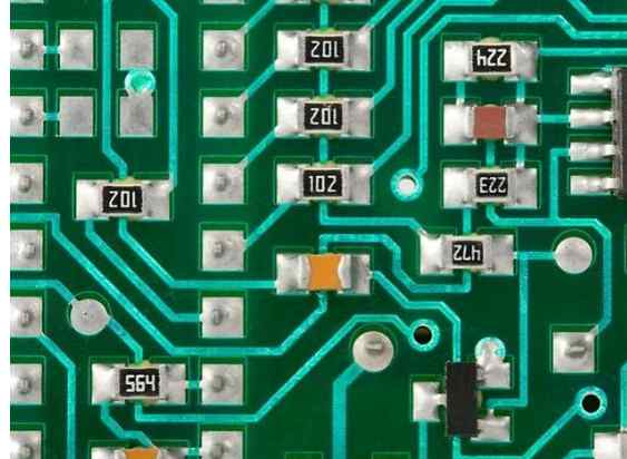
The first is the preferred solution. The outer layer of the PCB is all the strata, and the middle two layers are the signal/power layer. The power supply at the signal layer is routed with a wide wire, which allows the path impedance of the power supply current to be low, and the impedance of the signal microstrip path to be low. From an EMI control point of view, this is the best 4-layer PCB structure available. The outer layer of the second scheme takes the power supply and ground, and the middle two layers take the signal. Compared with the traditional 4-layer board, the improvement is less, and the interlayer impedance is as poor as the traditional 4-layer board.
To control the impedance of the cables, carefully place the cables under the copper islands of the power supply and ground. In addition, the power supply or copper-laying islands on the formation should be interconnected as much as possible to ensure DC and low frequency connectivity.
Six-ply plate
If the density of the components on the 4-ply plate is relatively high, it is better to use the 6-ply plate. However, the shielding effect of the electromagnetic field is not good enough for some laminated schemes in the design of 6-layer board, which has little effect on the reduction of the transient signal of the power busbar. Two examples are discussed below.
In the first case, the power supply and the ground are placed in the second and fifth layers respectively. Due to the high copper impedance of the power supply, it is very unfavorable to the control of common mode EMI radiation. However, from the point of view of impedance control of the signal, this method is very correct.
The second example places the power supply and ground in layers 3 and 4, respectively. This design solves the problem of copper-clad impedance of the power supply. Due to the poor electromagnetic shielding performance of layers 1 and 6, differential mode EMI is increased. If the number of signal wires on the two outer layers is minimal and the line length is very short (less than 1/20 of the highest harmonic wavelength of the signal), then this design can solve the differential mode EMI problem. The suppression of differential mode EMI is particularly good when the non-component and non-wireline areas on the outer layer are filled with copper and the copper-covered areas are grounded (at intervals of 1/20 wavelength). As mentioned above, the copper-laying area should be connected to multiple points of the internal connecting strata.

General purpose high performance 6-story board designs generally distribute layers 1 and 6 as strata, and layers 3 and 4 as power and ground. Because there are two layers of microstrip signal line between the power layer and the ground layer, EMI suppression ability is excellent. The drawback of this design is that there are only two layers of wiring. As described earlier, if the outer wiring is short and copper is laid in the non-wiring area, the same stacking can be achieved with a conventional 6-ply board.
Another 6-layer board layout is signal, ground, signal, power, ground, signal, which enables the environment required for advanced signal integrity design. The signal layer is adjacent to the grounding layer, and the power layer is paired with the grounding layer. Obviously, the downside is that the layers are stacked unevenly.
This usually causes problems in manufacturing. The solution to the problem is to fill all the blank areas of the third layer with copper. After filling with copper, if the copper coating density of the third layer is close to that of the power layer or grounding layer, this board can be loosely counted as a structurally balanced circuit board. The copper filling area must be connected to the power supply or grounded. The holes are still 1/20 wavelength apart, so you don't have to connect them everywhere, but ideally you should.
10-ply plate
Because the insulation between the layers is so thin, the impedance between layers of 10 or 12 boards is very low, and excellent signal integrity is expected as long as the layering and stacking are not problematic. It is difficult to process and manufacture 12-layer plates with a thickness of 62mil, and there are not many manufacturers capable of processing 12-layer plates.
Since there is always an insulating layer between the signal layer and the loop layer, it is not optimal to allocate the middle six layers to route the signal line in the 10-layer board design. In addition, it is important to have the signal layer adjacent to the loop layer, that is, the board layout is signal, ground, signal, signal, power, ground, signal, signal, signal, signal.
This design provides a good path for signal current and its loop current. The proper routing strategy is to route the first floor in the X direction, the third floor in the Y direction, the fourth floor in the X direction, and so on. Visually, Layers 1 and 3 are a pair of layers, Layers 4 and 7 are a pair of layers, and Layers 8 and 10 are the last pair of layers. When the direction of the line needs to be changed, the signal line on Level 1 should be changed by "through the hole" to Level 3. In practice, you may not always be able to do this, but as a design concept, try to follow it.
Similarly, when the line direction of the signal changes, it should go from layers 8 and 10 or from layers 4 to 7 by passing through holes. This wiring ensures the tightest coupling between the forward path and the loop of the signal. For example, if the signal is routed on the first layer and the loop is routed on the second layer and only on the second layer, then even if the signal on the first layer is transferred to the third layer by "through the hole", its loop is still in the second layer, thus maintaining the characteristics of low inductance, large capacitance and good electromagnetic shielding performance.


