
Professional PCB manufacturing and assembly
Building 6, Zone 3, Yuekang Road,Bao'an District, Shenzhen, China
+86-13923401642Mon.-Sat.08:00-20:00

During PCB processing, it is inevitable to encounter multiple defective products, which may be caused by machine errors or human factors. For example, there is sometimes an exception called a disconnected state. The reason is the specific analysis of the specific situation.
PCB processing
If the fracture state is a point distribution rather than a complete open circuit circle, it is called a point hole fracture, and some people call it a wedge hole fracture. The common reason is improper handling of the slag removal process. In the process of PCB processing, the scum removal process will first be treated with starter, and then a strong oxidant "permanganate" will be corroded. This process will remove scum and produce microporous structures. After the removal process, the remaining oxidant is removed by reducing agent, and the typical formula is treated with acid liquid.
Circuit board
After the treatment of the rubber residue, the problem of the residue of the rubber residue will no longer occur. Everyone often ignores the monitoring of the reducing acid solution, which may leave the oxidant on the hole wall. After the circuit board enters the chemical copper manufacturing process, it will be micro etched after being treated with pore forming agent. At this time, the residual oxidant is immersed in the acid again to peel the resin in the residual oxidant area, which is equivalent to destroying the pore forming agent.
The damaged pore wall will not react in the subsequent palladium colloid and chemical copper treatment, and copper precipitation will not occur in these areas. Of course, if the foundation is not firm, the electroplating copper will not completely cover it, and cause the dot hole to crack. This problem has occurred in many PCB factories when processing circuit boards. In the reduction step of the smear removal process, more attention should be paid to the monitoring of agents, which should be improved.
Every link in PCB processing requires us to strictly control, because chemical reactions sometimes occur slowly in the corners we do not pay attention to, thus damaging the entire circuit. In this puncture state, everyone should be vigilant.
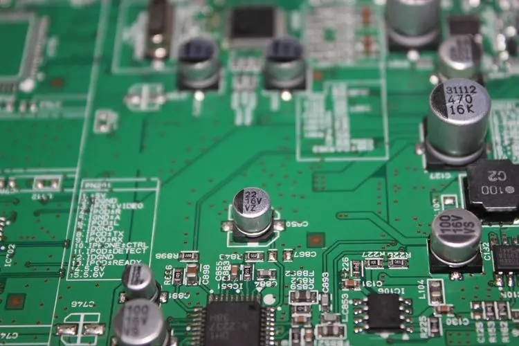
Bare boards (without parts on them) are also commonly referred to as "printed circuit board (PWB)". The base plate of the circuit board itself is made of insulating and heat insulating materials, which is not easy to bend. The visible small circuit material is copper foil. The copper foil initially covers the entire circuit board, but during the manufacturing process, part of the copper foil is etched, and the rest becomes a network composed of small wires. These lines, called conductor patterns or wiring, are used to provide circuit connections for components on a PCB.
Usually, the color of PCB is green or brown, which is the color of solder mask. It is an insulating protective layer, which can protect copper wires, prevent short circuit caused by wave crest PCB welding, and save solder. Screen printing is also printed on solder masks. Words and symbols (mostly white) are usually printed on the board to mark the position of each part on the board. Screen printed surfaces are also known as legend surfaces.
When the final product is made, integrated PCB circuits, transistors, diodes, passive components (such as resistors, capacitors, connectors, etc.) and various other electronic components will be installed on it. Through wire connection, electronic signal connection and application function can be formed.


Telegram
Just upload Gerber files, BOM files and design files, and the KINGFORD team will provide a complete quotation within 24h.