

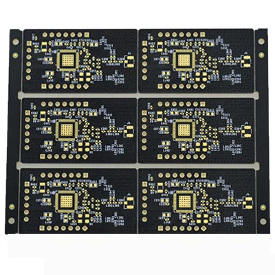
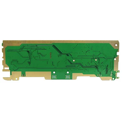
Name: 4-layer FR4PCB
Material: Fr4
Plate thickness: 1.6mm
Surface treatment: HASL lead free
Copper thickness: 1OZ
Minimum line: 6 million
Minimum hole: 0.3MM
Application: Router
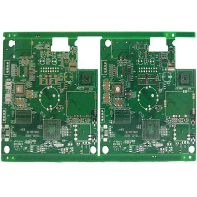
Name: 10-layer FR4 PCB
Layers: 10 layers
Material: FR-4
Plate thickness: 2.0mm
Board used: FR4
Surface Treatment: Immersion Gold
Minimum aperture: 0.1mm
Outer line width/line spacing: 4/4mil
Inner line width/line spacing: 5/5mil
Solder mask character color: black oil white
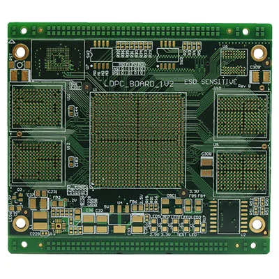
10-layer impedance plug hole PCB circuit board
Name: 10-layer impedance plug hole PCB circuit board
Application industry: consumer electronics
Application Product: Solid State Drive
Layers: 10
Special process: impedance line, resin plug hole, yin and yang copper
Surface Treatment: Immersion Gold
Aspect ratio: 8:1
Material: FR4
Outer line width/line spacing: 4/4mil
Inner layer line width/line spacing: 5/3.5mil
Plate thickness: 2.0mm
Minimum aperture: 0.25mm
6-layer impedance control immersion gold PCB circuit board
Name: 6-layer impedance control immersion gold PCB circuit board
Application industry: consumer electronics
Application product: handheld terminal
Layers: 6
Special process: impedance line
Surface Treatment: Immersion Gold
Material: FR4
Outer line width/line spacing: 3.5/4mil
Inner layer line width/line spacing: 4/4mil
Plate thickness: 1.6mm
Minimum aperture: 0.25mm
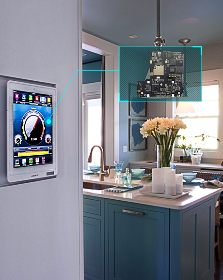
4-layer impedance control fine circuit immersion gold PCB circuit board
Name: 4-layer impedance control fine circuit immersion gold PCB circuit board
Application industry: consumer electronics
Application product: smart home control panel
Layers: 4
Special process: impedance line
Surface Treatment: Immersion Gold
Material: FR4
Outer line width/line spacing: 3.5/3.5mil
Inner layer line width/line spacing: 3.5/3mil
Plate thickness: 0.8mm
Minimum aperture: 0.2mm
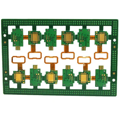
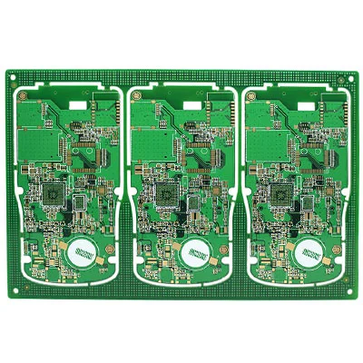
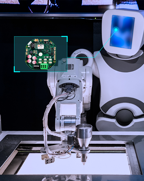
4-layer FPC+FR4 soft and hard combination PCB circuit board
Name: 4-layer FPC+FR4 rigid-flex PCB circuit board
Application industry: consumer electronics
Application product: wearable device
Layers: 4
Special process: soft and hard board
Surface Treatment: Immersion Gold
Material: FR4 + FPC
Outer line width/line spacing: 4/3.5mil
Inner layer line width/line spacing: 5/4mil
Plate thickness: 0.5mm
Minimum aperture: 0.2mm
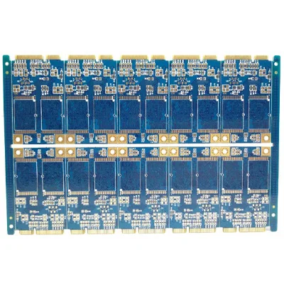
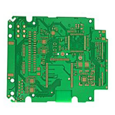
4-layer immersion gold PCB circuit board
Name: 4-layer immersion gold PCB circuit board
Application industry: consumer electronics
Application Products: Solid State Drive SSD
Layers: 4
Surface Treatment: Immersion Gold
Material: FR4
Outer line width/line spacing: 6/4mil
Inner layer line width/line spacing: 6/4mil
Plate thickness: 1.1mm
Minimum aperture: 0.3mm
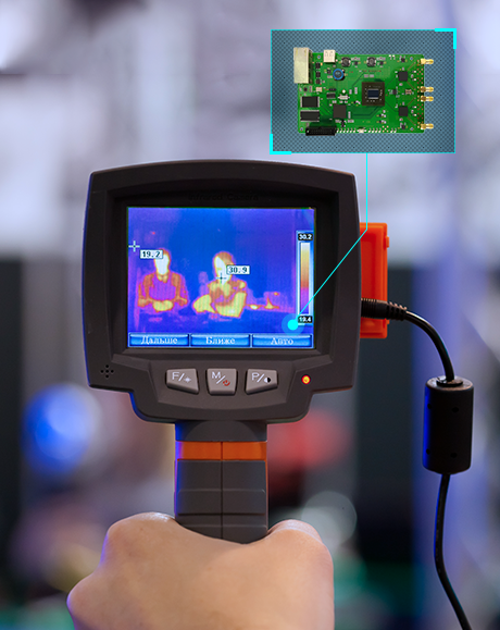
4-layer tin spray impedance circuit board
Name: 4-layer tin-sprayed impedance circuit board
Application industry: automotive electronics
Application product: vehicle GPS positioning system
Layers: 4
Special process: impedance board
Surface treatment: lead-free spray tin
Material: FR4
Outer line width/line spacing: 4/4mil
Inner layer line width/line spacing: 7/6mil
Plate thickness: 1.0mm
Minimum aperture: 0.2mm
- PCB Manufacturing Equipment
- PCB manufacturing capability

PCB Drilling machine

PCB pattern plating line

PCB solder mask expose machine

PCB pattern expose machine

Strip film etching line

Solder mask screen silk print machine

Solder mask scrubbing line
")
PCB Flying Probe Test (FPT)

Fully automatic exposure machine
| Standard PCB Production Capability | |
| Feature | Capability |
| Quality Grade | Standard IPC 2 |
| Number of Layers | 1 - 32layers |
| Order Quantity | 1pcs - 10,000,000 pcs |
| Build Time | 2days - 5weeks (Expedited Service) |
| Material | FR-4 Standard Tg 150°C, FR4-High Tg 170°C, FR4-High-Tg 180°C, FR4-Halogen-free, FR4-Halogen-free & High-Tg |
| Board Size | Min 6*6mm | Max 600*700mm |
| Board size tolerance | ±0.1mm - ±0.3mm |
| Board Thickness | 0.4mm - 3.2mm |
| Board Thickness Tolerance | ±0.1mm - ±10% |
| Copper Weight | 0.5oz - 6.0oz |
| Inner Layer Copper Weight | 0.5oz - 2.0oz |
| Copper Thickness Tolerance | +0μm +20μm |
| Min Tracing/Spacing | 3mil/3mil |
| Solder Mask Sides | As per the file |
| Solder Mask Color | Green, White, Blue, Black, Red, Yellow |
| Silkscreen Sides | As per the file |
| Silkscreen Color | White, Blue, Black, Red, Yellow |
| Surface Finish | HASL - Hot Air Solder Leveling |
| Lead Free HASL - RoHS | |
| ENIG - Electroless Nickle/Immersion Gold - RoHS | |
| ENEPIG - Electroless Nickel Electroless Palladium Immersion Gold - RoHS | |
| Immersion Silver - RoHS | |
| Immersion Tin - RoHS | |
| OSP -Organic Solderability Preservatives - RoHS | |
| Min Annular Ring | 3mil |
| Min Drilling Hole Diameter | 6mil, 4mil-laser drill |
| Min Width of Cutout (NPTH) | 0.8mm |
| NPTH Hole Size Tolerance | ±.002" (±0.05mm) |
| Min Width of Slot Hole (PTH) | 0.6mm |
| PTH Hole Size Tolerance | ±.003" (±0.08mm) - ±4mil |
| Surface/Hole Plating Thickness | 20μm - 30μm |
| SM Tolerance (LPI) | .003" (0.075mm) |
| Aspect Ratio | 1.10 (hole size: board thickness) |
| Test | 10V - 250V, flying probe or testing fixture |
| Impedance tolerance | ±5% - ±10% |
| SMD Pitch | 0.2mm(8mil) |
| BGA Pitch | 0.2mm(8mil) |
| Chamfer of Gold Fingers | 20, 30, 45, 60 |
| Other Techniques | Gold fingers |
| Blind and Buried Holes | |
| peelable solder mask | |
| Edge plating | |
| Carbon Mask | |
| Kapton tape | |
| Countersink/counterbore hole | |
| Half-cut/Castellated hole | |
| Press fit hole | |
| Via tented/covered with resin | |
| Via plugged/filled with resin | |
| Via in pad | |
| Electrical Test | |

High-standard confidentiality measures, signing confidentiality agreements, and all documents exporting must be approved to ensure that 100% of documents are not leaked.

we provide 24-hour service and support, you will receive a reply to your question within 2 hours and a quotation within 24 hours.

We can provide you with high frequency, high TG, high CTI, buried blind via, aluminum based PCB manufacturing, the quality is fully compliant with IPC 610-D standard, testing and quality assurance

With more than 20 years of industry experience, technology and production capacity are constantly increasing, and we can provide one-stop services from standard PCB to HDI PCB, high frequency and high...

Kingford has stable material suppliers with ten years of cooperation, such as Shengyi Technology, ITEQ, ROGERS, AGC, DUPONT, Doosan, Mitsubishi, etc.
FR4 Materials and PropertiesFR4 is a standard for glass fiber reinforced epoxy compounds defined by ...
We manufacture a 10-layer FR4 rigid PCB with a board thickness of 1.6 mm and a copper thickness of 1...
Classification: There are two types of storage media for solid-state drives, one is to use flash ...
Product introductionA handheld terminal refers to a portable data processing terminal with the follo...
All the node control modules of the smart home system are connected with the system information cont...
Wearable devices should have two most important characteristics: one is long-term wearability, and t...


Telegram