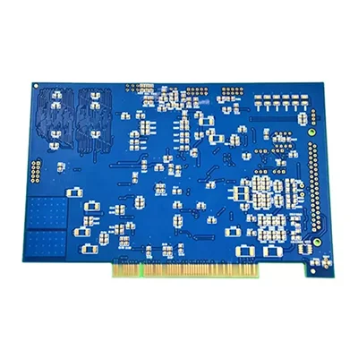
Multilayer Goldfinger Mainboard Control PCB
Name: Multilayer Gold Finger Mainboard Control PCB
Type: Multilayer circuit board
Layers: 6 layers
Substrate: FR4, Aluminum, High Tg FR4
Copper Thickness: 0.5-1 oz
Plate thickness: 0.4-4.0mm
minute. Hole size: 0.15-0.2mm
minute. Line width: 0.1-0.3mm
minute. Line spacing: 0.1-0.3mm
Surface treatment: Immersion gold, spray tin, gold finger
Solder Mask: Green
Applicable to: LED, mobile phone, computer, air conditioner
Certification: ISO-9001, ISO-14001, RoHS
Weight: 0.01-5KG
Application: Electronic Equipment
Detailed processing of PCB Gold Finger:
1) For PCB boards that need to be plugged in frequently, golden fingers generally need to be plated hard to increase the abrasion resistance of the golden finger.
2) Golden fingers need to fall backwards, generally 45 °, other angles such as 20 °, 30 °, etc. If there is no backward in the design, there is a problem. As shown in the figure below, the arrow shows 45 ° backward angle:
3) Golden fingers need to do a whole piece of welding windows. PIN does not need to open steel nets;
4) The minimum distance between Shenxi and Shenyin pads is 14 mil. It is recommended that the pads are more than 1mm from the finger position, including over -the -hole pads;
5) Do not apply copper on the surface of the golden finger.
Name: Multilayer Gold Finger Mainboard Control PCB
Type: Multilayer circuit board
Layers: 6 layers
Substrate: FR4, Aluminum, High Tg FR4
Copper Thickness: 0.5-1 oz
Plate thickness: 0.4-4.0mm
minute. Hole size: 0.15-0.2mm
minute. Line width: 0.1-0.3mm
minute. Line spacing: 0.1-0.3mm
Surface treatment: Immersion gold, spray tin, gold finger
Solder Mask: Green
Applicable to: LED, mobile phone, computer, air conditioner
Certification: ISO-9001, ISO-14001, RoHS
Weight: 0.01-5KG
Application: Electronic Equipment
- Previous:FR4 double-sided gold finger PCB
- Next:No


