

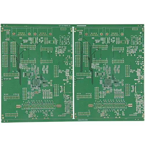
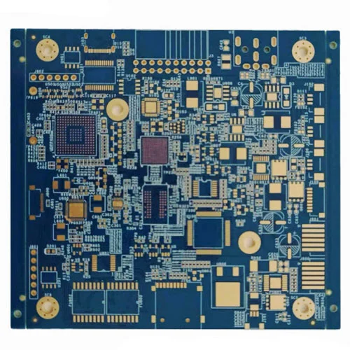
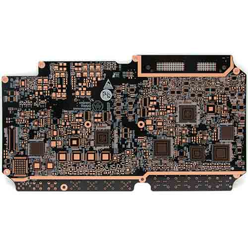
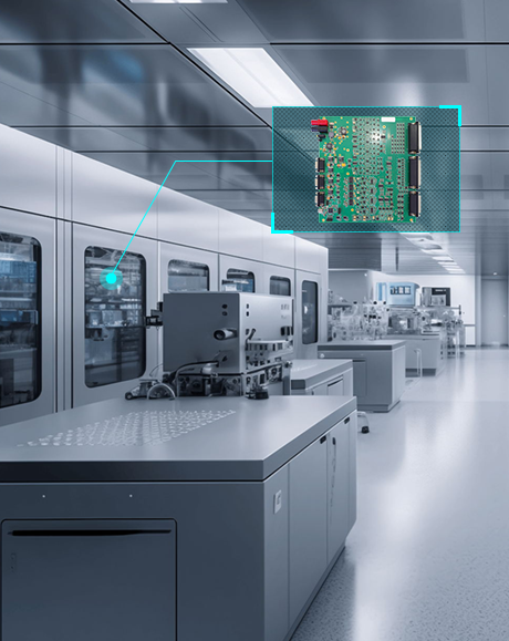
Name: Car driving recorder HDI PCB
Tier: 1+6+1
Sheet: EM825
Plate thickness: 1.6mm
Size: 242mm*165mm
Minimum blind hole: 0.1mm
Min Buried Via: 0.25mm
Minimum line width: 0.088mm
Minimum line spacing: 0.087mm
Surface Treatment: Immersion Gold
Outline tolerance: +/-0.1mm
Special requirements: L3-L6 resin plug holes
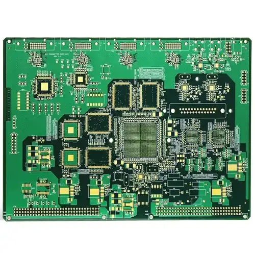
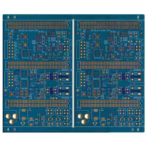
10-layer 1-stage HDI communication PCB
Name: 10-layer 1-stage HDI communication PCB
Layers: 1+8+1
Sheet: FR4 Tg170
Plate thickness: 1.2mm
Panel size: 110.8*94.8mm/4
Outer copper thickness: 35μm
Inner layer copper thickness: 18μm
Minimum through hole: 0.20mm
Minimum blind hole: 0.10mm
Minimum BGA: 0.20mm
Line width and line spacing: 2.5/2.2mil
Surface Treatment: Immersion Gold 2μ''+OSP
Application field: communication
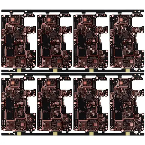
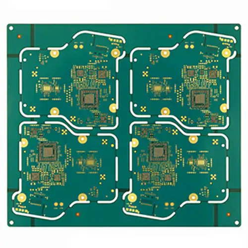
6L 2+N+2 HDI Communication PCB
Name: 6L 2+N+2 HDI Communication PCB
Model : 2+N+2 HDI Communication PCB
Layers : 6Layers
Material: IT150
Construction : 2+2+2 HDI PCB
Finished Thickness: 0.8mm
Copper Thickness: 0.5OZ
Color : Green/White
Surface Treatment: Immersion Gold+OSP
Min Trace / Space: 3mil/3mil
Min Hole: Laser Hole 0.1mm
Application : Communication HDI PCB
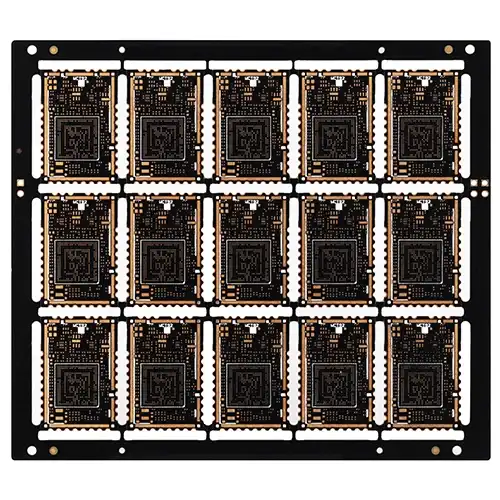
Name: 6L 2+N+2 HDI WiFi Module PCB
Layers : 6Layers
Material:FR4 Tg170
Construction : 2+2+2 HDI PCB
Finished Thickness: 0.8mm
Copper Thickness: 1OZ
Color : Black/White
Surface Treatment: Immersion Gold+OSP
Min Trace / Space: 3mil/3mil
Min Hole: Laser Hole 0.1mm
Application : WiFi module PCB
Name: 6-layer 1-stage HDI PCB
Layers: 1+4+1
Sheet: FR4 Tg150
Plate thickness: 1.6mm
Panel size 105*95mm/1
Outer copper thickness: 35μm
Inner layer copper thickness: 30μm
Minimum through hole: 0.20mm
Minimum blind hole: 0.10mm
Minimum BGA: 0.20mm
Line width line spacing: 3/3mil
Surface Treatment: Immersion Gold 2μ''+OSP
Application field: industrial control
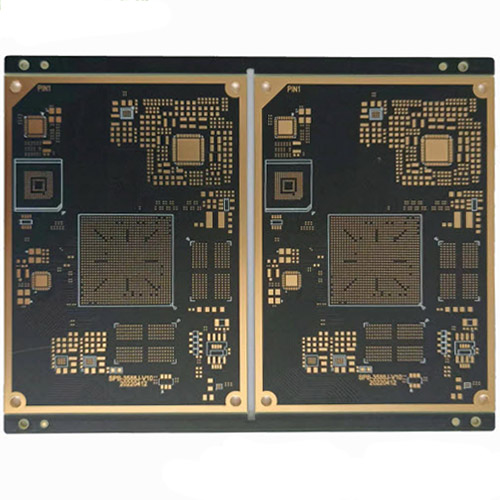
Name: 10-layer 3-stage HDI PCB
Layers: 3+4+3
Sheet: FR4 Tg170
Plate thickness: 1.2mm
Panel size: 126*118mm/4
Outer copper thickness: 35μm
Inner layer copper thickness: 18μm
Minimum through hole: 0.20mm
Minimum blind hole: 0.10mm
Minimum BGA: 0.25mm
Line width and spacing: 2.8/3.2mil
Surface Treatment: Immersion Gold 2μ''+OSP
Name: 10-layer 1-level HDI pcb
Layers: 1+8+1
Sheet: FR4 Tg170
Plate thickness: 1.6mm
Panel size: 121.6*95mm/2
Outer copper thickness: 1OZ
Inner layer copper thickness: 1OZ
Minimum through hole: 0.20mm
Minimum blind hole: 0.10mm
Minimum BGA: 0.25mm
Line width line spacing: 3/2.7mil
Surface Treatment: Immersion Gold 2μ''
Blind hole process: hole filling and electroplating
Name: 2+N+2 HDI ITEQ PCB 6L PCB
Model : 6L 2+N+2 HDI PCB
Material: ITEQ IT150
Layer: 6L 2+N+2 HDI
Color: Black/White
Finished Thickness: 1.0m
Copper Thickness: inner1OZ outer0.5OZ
Surface Treatment :Immersion Gold +OSP
Min Trace / Space: 2.5mil/2.5mil
Min Hole: Mechanical hole 0.2mm, Laser Hole 0.1mm
Application: Communication pcb
Communication equipment 2-stage HDI PCB board
Name: Automotive communication second-order HDI board
Plate: S1000-2M
Layers: 14L
Material: ISOLA
Plate thickness: 1.6±0.16mm
Minimum aperture laser hole: 0.10mm
Mechanical hole: 0.20mm
Minimum track/spacing: 75/75um
Minimum plate thickness and porosity: 8:1
Special process: 2 laser drilling, 3 pressing, second-order HDI board
Use: vehicle communication
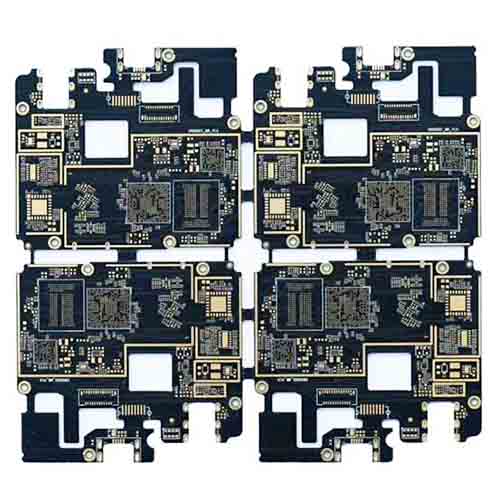
Twelve-layer second-order board
name: Twelve-layer second-order board
Plate: FR4
Layers: 12L
Material: ISOLA
Plate Thickness: 2.0mm
Copper thickness of inner and outer layers: 1oz
Minimum hole diameter: 0.1mm
Surface Treatment: Immersion Gold
Line width: 0.1mm
Line distance: 0.1mm
BGA pad: 0.15mm
Special craftsmanship: second stage
Use: consumer electronics
- PCB Manufacturing Equipment
- HDI PCB Capability

PCB Drilling machine

PCB pattern plating line

PCB solder mask expose machine

PCB pattern expose machine

Strip film etching line

Solder mask screen silk print machine

Solder mask scrubbing line
")
PCB Flying Probe Test (FPT)

Fully automatic exposure machine
| HDI (High Density Interconnect) PCB Process Capability | ||
| Item | batch | Template |
| layers | 4-16 Layers | 4-24 Layers |
| Plate thickness range | 0.6-3.2mm | 0.4-6.0mm |
| highest order | 4+N+4 | Any layer innterconnected |
| Minimum laser hole | 4mil (0.1mm) | 3mil (0.075mm) |
| Laser process | CO2 Laser Machine | CO2 Laser Machine |
| Tg value | 140/150/170°C | 140/150/170°C |
| hole copper | 12-18μm | 12-18μm |
| Impedance tolerance | +/-10% | +/-7% |
| interlayer alignment | +/-3mil | +/-2mil |
| Solder Mask Alignment | +/-2mil | +/-1mil |
| Minimum line width/line spacing | 2.5/2.5mil | 2.0/2.0mil |
| Smallest grommet | 2.5mil | 2.5mil |
| Minimum through hole | 8mil (0.2mm) | 6mil(0.15mm) |
| smallest micropore | 4.0mil | 3.0mil |
| Minimum media thickness | 3.0mil | 2.0mil |
| Minimum pad | 12mil | 10mil |
| Micropore Aperture Aspect Ratio | 1:1 | 1:2:1 |

High-standard confidentiality measures, signing confidentiality agreements, and all documents exporting must be approved to ensure that 100% of documents are not leaked.

we provide 24-hour service and support, you will receive a reply to your question within 2 hours and a quotation within 24 hours.

We can provide you with high frequency, high TG, high CTI, buried blind via, aluminum based PCB manufacturing, the quality is fully compliant with IPC 610-D standard, testing and quality assurance

With more than 20 years of industry experience, technology and production capacity are constantly increasing, and we can provide one-stop services from standard PCB to HDI PCB, high frequency and high...

Kingford has stable material suppliers with ten years of cooperation, such as Shengyi Technology, ITEQ, ROGERS, AGC, DUPONT, Doosan, Mitsubishi, etc.
Kingford provides Car driving recorder HDI PCB services. This is a PCBA one-stop assembly factory wi...
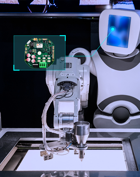
We support 10-layer 1-stage HDI communication PCB business,Kingford is a professional one-stop PCBA ...
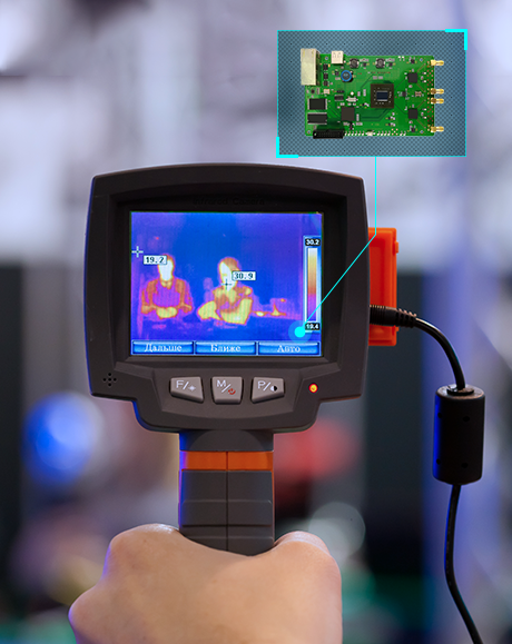
Kingford supports 6L 2+N+2 HDI Communication PCB business, we are a professional PCBA one-stop assem...
We provide 6L 2+N+2 HDI WiFi Module PCB services. Kingford is your one stop turnkey PCB assembly fac...
We support 6-layer 1-stage HDI PCB business, Kingford is a professional one-stop PCBA service factor...
Kingford provides 10-layer 3-stage HDI PCB services. This is a PCBA one-stop assembly factory with s...

We have robust quality inspection procedures, and most importantly, a large number of satisfied customers is the greatest testimony to our success.
Yes, we provide high-density PCB manufacturing services, if you have any needs, please contact sales@kingfordpcb.com


Telegram