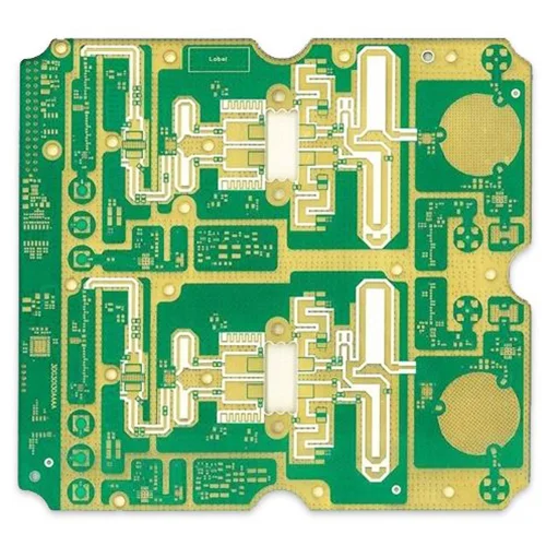
Lightwave Communications PCB Board
Name: Lightwave Communications PCB Board
Layers: 6L
material: TU872+R4350B
Board Thicknes: 1.8 mm
Copper Thicknes: 35/35/35/35um
Smallest Hole Diameter: 0.20mm
Surface Treatment: ENIG(2U'')
Technical Feature: Vacuum Plugging, Blind buried via
Applications
Ground receiving equipment
High-speed circuits are essential to increase the bandwidth for transmitting and switching voice/video/data over fiber optic networks. Due to the explosion in Internet traffic, the growing demand for bit rates has driven engineers to develop integrated circuits with performance approaching 100 Gb/s. Commercial lightwave products using high-speed circuits of 10 Gb/s and higher are readily available. High-Speed Circuits for Lightwave Communication provides the latest information on circuit design, measurement results, applications, and product development. It covers electronic and optoelectronic circuits for transmission, reception and crosspoint switching. These circuits are implemented using a variety of state-of-the-art IC technologies, including Si BJT, GaAs MESFET, HEMT, HBT, and InP HEMT and HBT.
Name: Lightwave Communications PCB Board
Layers: 6L
material: TU872+R4350B
Board Thicknes: 1.8 mm
Copper Thicknes: 35/35/35/35um
Smallest Hole Diameter: 0.20mm
Surface Treatment: ENIG(2U'')
Technical Feature: Vacuum Plugging, Blind buried via
Applications
Ground receiving equipment
- Previous:High Frequency Hybrid PCB Board
- Next:No


