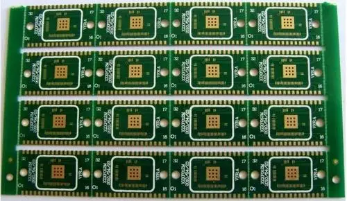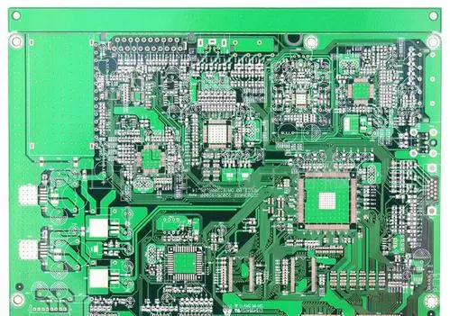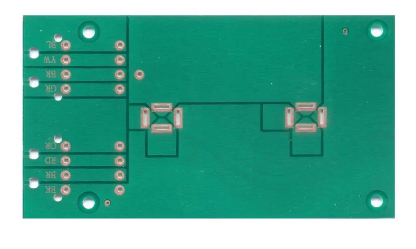
The micro assembly technology of SMT proofing and small batch processing is actually a comprehensive technology that uses micro welding and processing on high-density multilayer interconnection substrates to assemble various micro components that make up electronic circuits to form micro electronic products.
1、 Multichip module
The multi chip module in the SMT package is a high-tech electronic product derived and developed on the basis of hybrid integrated circuits. This technology integrates multiple LSI and VLSI chips on a hybrid multilayer interconnection substrate with high density, and then encapsulates them in a shell. It is a highly hybrid integrated module. SMT proofing small batch processing MCM chip interconnection and assembly technology is to assemble components and devices on MCM substrate in a specific connection mode, and then install the substrate for assembling components in the package to form a multi-functional MCM module. MCM chip interconnection and assembly technology includes: chip to substrate bonding, chip to substrate electrical connection, substrate to housing physical connection and electrical connection.
2、 Flip chip FC technology

SMT proofing small batch processing flip chip technology is to realize the interconnection between the chip and the circuit board through the bumps on the chip. Generally, chips are placed on circuit boards in reverse. Gold wire bonding technology generally uses the surrounding parts of the chip, while flip chip solder bump technology uses the entire chip surface, which can make flip chip technology have higher packaging density, thus reducing the size of the device. The flip chip technology in SMT labor package includes: solder paste flip chip assembly process, bonding method of solder column bump flip chip, and controlled collapse connection C4 technology.
SMT chip processing
3、 Package stacking
The appearance of PoP stack assembly technology in SMT labor and material package blurs the boundary between primary packaging and secondary assembly, which not only improves the logic operation function and storage space, but also provides the possibility for the end user to freely choose the device combination, thus controlling the production cost. The main function of PoP package is to integrate high-density digital or mixed signal logic devices in the bottom package and high-density or combined memory devices in the top package.
4、 Photoelectric interconnection technology
1. Photoelectric board level packaging SMT proofing small batch processing of photoelectric board level packaging is to integrate photoelectric devices and electronic packaging to form a new board level packaging. This board level package can be seen as a special multi chip module including pcb devices such as optical circuit substrate, optical devices, optical waveguide, optical fiber, optical connector, etc.
2. Optoelectronic components and modules Optoelectronic components and modules Optoelectronic components and modules Optoelectronic circuit components or modules formed by optoelectronic packaging technology can be made on one substrate with copper conductors for transmitting electrical signals and optical paths for transmitting optical signals.
3. The hierarchical structure of optical circuit board assembly The optical circuit assembly is generally composed of 6 layers. Chip level, device level, MCM level, board level, component level and system level.


