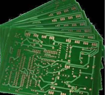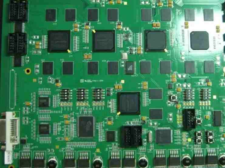
It has been proved that the reliability of electronic equipment will be adversely affected even if the circuit diagram is designed correctly and the printed circuit board is not designed properly
At present, the printed circuit board is still used as the main assembly method for all kinds of electronic equipment and systems. It has been proved that the reliability of electronic equipment will be adversely affected even if the circuit diagram is designed correctly and the printed circuit board is not designed properly. For example, if two thin parallel lines on a printed board are close together, there will be a delay in the signal waveform, creating reflected noise at the end of the transmission line. Therefore, in the design of printed circuit board, should pay attention to the use of correct methods.
Ground wire design
Grounding is an important method to control interference in electronic equipment. If the grounding and shielding can be correctly combined, most interference problems can be solved. The structure of ground wire in electronic equipment is generally systematic, housing ground (shield ground), digital ground (logical) and analog ground. The following points should be noted in the design of ground wire:

1, the correct choice of single point grounding and multi-point grounding
In low-frequency circuit, the working frequency of the signal is less than 1MHz, and the inductance between the wiring and the device has little influence, while the circulation formed by the grounding circuit has great influence on the interference, so a point grounding should be used. When the signal working frequency is greater than 10MHz, the ground impedance becomes large. In this case, the ground impedance should be reduced as much as possible and the nearest multipoint grounding should be used. When the operating frequency ranges from 1 MHZ to 10 MHZ, if a one-point grounding is used, the length of the ground wire should not exceed 1/20 of the wavelength. Otherwise, the multi-point grounding method should be used.
2. Separate the digital circuit from the analog circuit
Both high-speed logic circuit and linear circuit on the circuit board should be separated as far as possible, and the ground wire of the two should not be mixed, respectively connected with the ground wire of the power supply end. The ground area of the linear circuit should be increased as much as possible.
3. Make the ground wire as thick as possible
If the grounding wire is very fine, the grounding potential will change with the change of the current, resulting in the timing signal level of the electronic equipment is unstable, and the anti-noise performance deteriorates. Therefore, the ground wire should be as thick as possible, so that it can pass through the three allowable current located in the printed circuit board. If possible, the ground cable should be wider than 3mm.
4, the ground wire to form a closed-loop road
When designing the ground system of printed circuit board composed only of digital circuit, making the ground wire as a closed loop can obviously improve the anti-noise ability. The reason is that there are many integrated circuit components on the printed circuit board, especially in the case of power consumption of components, due to the limitation of the thickness of the grounding wire, will produce a large potential difference on the ground junction, causing the decrease of anti-noise ability, if the grounding structure into a loop, it will reduce the potential difference, improve the anti-noise ability of electronic equipment.
Electromagnetic compatibility design
Electromagnetic compatibility refers to the ability of electronic devices to work harmoniously and efficiently in various electromagnetic environments. The purpose of EMC design is to enable electronic equipment not only to suppress all kinds of external interference, so that electronic equipment can work properly in a specific electromagnetic environment, but also to reduce the electromagnetic interference of electronic equipment itself to other electronic equipment.
1. Choose a reasonable wire width
The inductance of the printed wire should be reduced as much as possible because the impulse interference of the transient current on the printed wire is mainly caused by the inductance component of the printed wire. The inductance of printed wire is proportional to its length and inversely proportional to its width, so a short and fine wire is advantageous to restrain interference. The signal lines of clock leads, line drivers, or bus drivers often carry large transient currents, and printed wires should be kept as short as possible. For discrete component circuit, printed wire width in about 1.5mm, you can fully meet the requirements; For integrated circuits, the printed wire width can be selected between 0.2 and 1.0mm.
2. Adopt the correct wiring strategy
The use of equal wiring can reduce the inductance of the wire, but the mutual inductance and distributed capacitance between the wires will increase. If the layout allows, it is better to use the zigzag network wiring structure. The specific method is that one side of the printed board is wired horizontally, the other side is wired vertically, and then the metal holes are connected at the cross holes.
In order to suppress the cross talk between printed board wires, in the design of wiring should be as far as possible to avoid long distance equal routing, as far as possible to open the distance between lines, signal lines and ground and power lines as far as possible do not cross. Crosstalk can be effectively suppressed by installing a printed line between some signal lines which are very sensitive to interference.
In order to avoid the electromagnetic radiation generated by the high frequency signal through the printed wire, the following points should also be paid attention to when the printed circuit board wiring:
● As far as possible to reduce the discontinuity of printed wire, such as wire width do not mutate, wire corner should be greater than 90 degrees to prohibit circular line, etc.
● The clock signal lead is most likely to produce electromagnetic radiation interference, when the wire should be close to the ground circuit, the driver should be next to the connector.
● The bus driver should be close to the bus it is intended to drive. For leads that leave the printed circuit board, the driver should be close to the connector.
● The wiring of the data bus should be sandwiched between each two signal wires a signal ground wire. It is best to place the ground loop close to the least important address lead, as the latter often carries high frequency current.
● When arranging high speed, medium speed and low speed logic circuits on the printed board, the devices should be arranged as shown in Figure 1.


