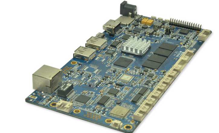
After the development of the past few years and the impact of the post-epidemic era, the basic pattern of PCB circuit board industry gradually emerged, forming an industrial cluster led by the electronic industry in the Pearl River Delta, the Yangtze River Delta and the Bohai Rim. From the current situation, only our country has recovered the supply of products in a short time, accelerating the trend of domestic replacement of PCB industry.
In addition, according to the forecast of related industry research institute, because of the advantages of labor, resources, policies and other aspects, our domestic PCB industry has developed rapidly, so far it has been called the world's largest production base. Based on the rising momentum of industrial increment from 2016 to 2020, which is higher than the compound annual growth rate of 2.77 of global output value in the same period, China's PCB industry is highly likely to reach the $40 billion mark in 2022.
There are more than 2,000 PCB industry enterprises in the country, which can be imagined how cruel the competition is, and it is a fierce competition in the "field of cultivation".
It is important for pcb manufacturers to share that pcba machining quality is very important, so PCBA designers need to consider this from the beginning. In some treatments, the quality of normal operation is flawed and it is easy to damage solder joints or electronic materials of machined SMT components if the initial design sketch is not suitable.
pcb manufacturers share that pcba processing should pay attention to these points:
1. BGA, chip capacitors, crystal oscillators and other stress-sensitive equipment are easily damaged by machinery or high temperature. Therefore, pcb manufacturers believe that when designing or reinforcing equipment, they should be placed on PCB boards with higher hardness, or use certain methods to avoid pcba processing.
2. When pcba processes components, it is necessary to arrange sensitive electronic components on PCB with higher stiffness. For example, in order to avoid damaging the sensitive electronic components of the PCB board during assembly, the connector that holds the PCB board and the mother board should be placed on the side of the PCB sub-board and should not be too small to the screw hole, more than 10 mm.
3.pcb manufacturer reminds that in order to avoid stress cracking of BGA solder joints, please avoid placing the BGA layout in the pcba processing and assembly process where it is easy to bend. The poor design of the BGA can easily cause the solder joints to crack if the board is held with one hand.
The above three points are mainly based on pcb manufacturers over the years of research and development and design published some discussion. In addition, it is important to reduce the pressure of assembly, adopt appropriate methods and tools, strengthen personnel training, and standardize the operation.
With the continuous development of electronic products, the frequency of various equipment failures is greatly increased, and the requirements for maintenance personnel are also constantly improving, especially for the maintenance personnel who just contact the circuit board. Many people do not know how to start at the beginning, and do not know how to learn. In fact, if you want to learn the maintenance of pcb board well, you need several electrical and modular electrical foundations.
pcb board schematic blueprint, the realization of the circuit user needs the function. The design of pcb board mainly refers to the design of the layout, the need for internal electronic components, metal wiring, through hole and external connection layout, electromagnetic protection, heat dissipation, crosstalk and other factors.
The following points should be paid attention to when repairing pcb board:
1. Before maintenance, first of all, we should do a good job of preventing static electricity, such as wearing clothes and shoes to prevent static electricity and wearing a wrist strap to prevent static electricity. The maintenance table should also be done to prevent electrostatic treatment, such as to prevent electrostatic table.
2, pay attention to electricity, including the circuit board to take into account the bearing capacity of the pcb circuit board.
3, when you need to contact strong electricity, pay attention to the human body, do a good job of strong electricity prevention measures.
Through the extraction and partial modification of the technical data files, the process of pcb board copying can realize the rapid updating and upgrading of various types of electronic products and secondary development. According to the document drawing and schematic diagram extracted from the board, it can be upgraded and optimized!

Circuit board push-back steps:
1. Record details about the pcb board
Get a pcb board, to record on the paper the model, parameters, position of all components, especially the direction of diode, three-stage tube, IC notch direction. You can use a digital camera to take two photos of the location of the device. A lot of circuit board copy board grade higher diode transistor some do not pay attention to see.
2. Scan the image
Remove all the components and remove the tin from the PAD hole. The pcb board is cleaned with alcohol and placed in a scanner, which scans with slightly higher pixels to get a sharper image. Then the top layer and the bottom layer are lightly polished with water gauze paper until the copper film is shiny. Then the two layers are swept in color by starting PS in the scanner.
3. Adjust and correct the image
Adjust the contrast and brightness of the canvas so that the part with copper film is in strong contrast with the part without copper film, then turn the subdrawing to black and white, check whether the lines of the circuit board copy board are clear, if not, repeat this step.
4. Check the position overlap
The two BMP files are converted into PROTEL files respectively, and two layers are transferred into PROTEL. If the positions of PAD and VIA after two layers are basically identical, it indicates that the previous steps have been done well. If there is any deviation, repeat the third step. So pcb board copy board is a very patient work, because a little problem will affect the quality and board copy board after the matching degree.
5. Draw layers
Convert the BMP of the TOP layer to the TOP PCB, be careful to convert to the SILK layer, which is the yellow layer, then you trace the line on the TOP layer and place the components according to the drawing. Delete the SILK layer when you are done. Repeat until all layers are drawn.
Step 8 Test
Test copy board electronic technology performance is the same as pcb board original board. If it's one, it's really done.


