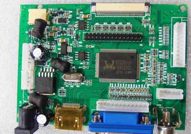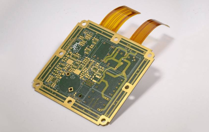
1, printed wire width selection basis: the minimum width of the printed wire is related to the size of the current flowing through the wire: the wire width is too small, the resistance of the printed wire is large, the voltage drop on the line is large, affecting the performance of the circuit, the wire width is too wide, the wiring density is not high, the board area increases, in addition to increasing the cost, it is not conducive to miniaturization. If the current load is calculated at 20A/ square millimeter, when the thickness of copper coated foil is 0.5MM, (generally so much), the current load of 1MM(about 40MIL) line width is 1A, therefore, the line width of 1 -- 2.54MM(40 -- 100MIL) can meet the general application requirements, the ground wire and power supply on the high power equipment board, According to the power size, the line width can be appropriately increased, and in the digital circuit with low power, in order to improve the wiring density, the minimum line width of 0.254 -- 1.27MM(10 -- 15MIL) can be satisfied. In the same circuit board, the power cord. Ground wire is thicker than signal wire.
2. Line spacing: When it is 1.5MM(about 60MIL), the insulation resistance between the wires is greater than 20M ohms, and the maximum voltage between the wires is up to 300V. When the spacing between the wires is 1MM(40MIL), the maximum voltage between the wires is 200V. Therefore, on the PCB board of medium and low voltage (the voltage between the wires is not more than 200V), Line spacing of 1.0 -- 1.5MM (40 -- 60MIL) in low-voltage circuits, such as digital circuit systems, do not have to consider the breakdown voltage, as long as the production process allo0ws, can be very small.
3, pad: for 1/8W resistance, the diameter of the pad lead is 28MIL is enough, and for 1/2W, the diameter is 32MIL, the lead hole is large, the width of the copper ring of the pad is relatively reduced, resulting in the adhesion of the pad decreased. Easy to fall off, lead hole is too small, the component is difficult to install.
4. Draw the circuit frame: the shortest distance between the frame line and the element pin pad should not be less than 2MM, (generally 5MM is more reasonable), otherwise it is difficult to cut the material.
5. Component layout principle: A: General principle: In PCB design, if the circuit system exists both digital circuit and analog circuit. And large current circuit, must be separated layout, so that the system between the coupling to achieve a minimum in the same type of circuit, according to the signal flow and function, block, partition placed components.
6, input signal processing unit, output signal driving element should be close to the circuit board, so that the input and output signal line as short as possible, in order to reduce the input and output interference.
7, component placement direction: components can only be arranged along the horizontal and vertical directions. Otherwise, the plugin cannot be used
8, component spacing. For medium density board, small components, such as low-power resistor, capacitor, diode, and other discrete components, the spacing between each other is related to plug-in, welding process, wave welding, component spacing can be 50-100MIL(1.27 -- 2.54MM) manual can be larger, such as 100MIL, integrated circuit chip, Component spacing is typically 100 -- 150MIL.
9. When the potential difference between components is large, the spacing between components should be large enough to prevent discharge.
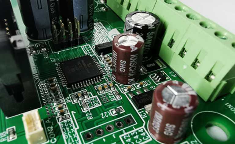
10, in the IC to remove the lotus capacitor should be close to the chip power supply ground pin. Otherwise the filtering will be bad. In the digital circuit, in order to ensure the reliable operation of the digital circuit system, the IC decoupling capacitor is placed between the power supply and the ground of each digital integrated circuit chip. The capacitance of lotus root removal capacitor is usually porcelain capacitor with a capacity of 0.01-0.1uF. The capacitance of lotus root removal capacitor is generally selected according to the reciprocal of the operating frequency F of the system. In addition, a 10UF capacitor and a 0.01UF ceramic capacitor shall be added between the power line and ground at the entrance of the circuit power supply.
11: The clockwise circuit element is as close as possible to the clock signal pin of the single chip microcomputer chip, so as to reduce the wire length of the clock circuit. And it's best not to run a line underneath

2. Reflow welding process with lead solder welding with lead and lead-free components mixed process
At present, the mixed assembly of lead and leadless electronic products with components is the widespread phenomenon in our country, namely, the mixing process of welding with lead solder and leadless components, referred to as the "mixed welding".
First, mixed welding mechanism
The use of lead solder welding with lead and lead-free components in mixed assembly welding there are two situations:
① Welding with lead solder and lead components. The welding process and mechanism are exactly the same as Sn-37Pb welding, and the main components of the intermetallic bonding layer (IMC) are Cu6Sn5 and Cu3Sn. Good compatibility.
② Solder with lead and lead-free components. The welding mechanism is basically the same as that of Sn-37Pb welding. However, because the welding end coating of lead-free components is very complicated, in addition to Sn, Sn-Ag-Cu, Ni-Au, Ni-Pd-Au plating, there are Sn-Cu, Sn-Bi alloy layer, Sn-Pb solder and different metals welding may be incompatible, affecting the reliability.
Two, the main characteristics of mixed welding and possible compatibility problems
Traditional Sn-37Pb solder is used for mixed assembly welding. The components to be welded in SMT include both lead and lead-free components. When lead-free components are welded with lead solder, the melting point of Sn-Pb solder is 183℃, the melting point of Sn of lead-free component welding end coating is 232℃, and the melting point of Sn-Ag-Cu of lead-free BGA welding ball is 217℃. The welding temperature of complex PCBA assembly plate may be higher. Although the material and melting point temperature are compatible when lead materials are welded with lead components, the welding temperature is increased due to SMT reflow welding. High temperatures may damage lead components and PCB substrates.
Compatibility problems may occur with lead and lead-free mixed welds as described below.
1. Sn plating element must be directed.
2. High temperature may damage component packaging and internal connections.
3. Adverse effects of high temperature on moisture sensitive elements.
4. High temperature may damage PCB.
5. Sn-Pb solder alloy is incompatible with lead-free element welding end coating (Sn-Bi element).
6, Sn-Pb solder alloy and lead-free PBGA, CSP ball alloy is incompatible
7. Incompatibility between various processes.
8. Incompatibility between various fluxes.
According to the above analysis, the requirements of mixed welding products from the beginning of the design should take into account the compatibility and reliability of mixed packaging, and make the process more detailed


