Hot air welding disc science
Many engineers who are responsible for Process or SMT technology in the factory will often come across solder empty, de-solder or cold solder of the circuit board components and other non-solder problems. No matter how to change the process conditions or how to adjust the furnace temperature of reflow welding, there is a certain proportion of tin can not be welded. What the hell is going on here?
Apart from the oxidation of components and circuit boards, it is found that a large part of such poor welding actually comes from the lack of layout design of circuit boards, and the most common is that a few welding feet of components are connected to a large area of copper, resulting in poor welding of these components after reflow welding. Some hand welded components may also cause false welding or cladding problems due to similar conditions, and some may even weld the components due to excessive heating.
In general PCB circuit design often need to lay a large area of copper foil for power (Vcc, Vdd or Vss) and Ground (GND, Ground). These large areas of copper foil will generally be directly connected to some control circuit (IC) and electronic components of the pin.

Unfortunately, if we want to heat these large areas of copper foil to the temperature of tin melting, it usually takes more time than the independent pad (that is, the heating will be slower), and the heat dissipation is faster. When one end of such a large area of copper foil wiring is connected to small components such as small resistance and capacitance, and the other end is not, it is easy to melt tin and solidification time is inconsistent and welding problems occur; If the temperature curve of reflow welding is not adjusted well and the preheating time is not enough, the welding feet of these components connected in large copper foil are easy to cause the problem of false welding because they cannot reach the tin melting temperature.
When manual welding (Hand Soldering), the welding feet of these components connected to a large piece of copper foil will be too fast because of heat dissipation, and can not be completed in the specified time. The most common adverse phenomenon is cladding welding, virtual welding, solder only welding on the component of the welding foot and not connected to the circuit board of the pad. From the appearance, the entire solder joint will form a ball; What is more, in order to weld the welding feet on the circuit board and constantly adjust the temperature of the iron, or heating for too long, so that the components exceed the heat resistant temperature and damage without knowing it.
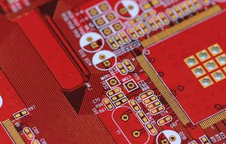
Since we know the problem points, we can have a solution. Generally, we will require the so-called Thermal Relief pad (hot air welding pad) design to solve the welding problems caused by the welding feet of large copper foil connecting components. As shown in the figure below, the wiring on the left does not use hot air welding pad, while the wiring on the right has adopted the connection mode of hot air welding pad. It can be seen that the contact area between the welding pad and large copper foil is only a few small lines, which can greatly limit the loss of temperature on the welding pad and achieve better welding effect.
Check your work
When you're struggling to put all the pieces together for manufacturing, it's easy to find problems at the end of a design project and be overwhelmed. Therefore, double and triple checking your design work at this stage can mean the difference between manufacturing success and failure.
To help complete the quality control process, we always recommend that you start with an Electrical Rule Check (ERC) and a Design Rule Check (DRC) to verify that your design fully meets all rules and constraints. With these two systems, you can easily check clearance width, line width, common manufacturing Settings, high speed requirements and short circuits.
When your ERC and DRC produce error-free results, it is recommended that you examine the wiring of each signal, from schematic to PCB, one signal line at a time in a way that carefully ensures that you are not missing any information. Also, use the probe and mask features of your design tools to ensure that your PCB layout materials match your schematics.


