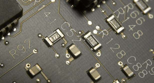
PCB laminatecharacteristics are the basis of RF and microwave PCB board performance. The available laminate types have different characteristics, including dielectric constant (aka k factor), tangent of loss Angle, and temperature coefficient. These factors all affect the performance of your RF and microwave PCB boards throughout their life cycle. These properties can be affected by a number of factors, including the thickness of the PCB material, the type of substrate used, and even the number of layers of the RF and microwave PCB board itself.
The most important factor when choosing a PCB laminate is to ensure that it is compatible with your RF and microwave PCB design requirements. For example, if you need high frequency performance, you may want to choose a material with a high dielectric constant, such as Rogers Core or Rogers 3705 PTFE laminates. However, if you do not require high frequency properties, a lower K-factor material (such as FR4) may be sufficient for your needs.
Rf and microwave PCB transmission lines and through holes
Transmission lines are used to carry radio frequency signals from one place to another. Transmission lines have different impedance values and can be classified according to their electrical length. Impedance is the resistance to current caused by inductance, capacitance, and other electrical characteristics. A transmission line usually consists of a single conductor or a pair of conductors (shielded or unshielded). The impedance of a transmission line depends on its physical length and operating frequency.

The main purpose of the transmission line is to reduce signal reflection during conversion between two devices on RF and microwave PCBS. To do this, you must ensure that there are no discontinuities in the line that could cause reflection or standing waves. This requires careful design planning when placing components on your RF and microwave PCB board layout and selecting the right transmission line design for your application.
There are three types of transmission lines: coaxial cable, microstrip line and trough line.
Coaxial cable
Coaxial cables are used in high-frequency applications up to 40 GHz because they can handle high currents over the entire bandwidth range with little loss. Coaxial cables are usually made of copper wire, but other RF and microwave PCB materials, such as silver plated copper, can be used, depending on the frequency band and power requirements of the application.
microstrip
Microstrip lines are the most commonly used transmission lines. It consists of a ground layer on one side of RF PCB laminate and an elevated signal route on the other side. The ground plane should be wider than the signal line, so there is no interaction between them. The dielectric layer should be at least 1/4 inch thick for millimeter wave frequencies and 1/2 inch thick for UHF or higher frequencies. At lower frequencies, you can use a thinner dielectric, such as FR-4 or Rogers 4350, without increased loss due to the edge field between the ground layer and the signal line.
Ribbon line
The strip line is similar to the microstrip line, except that it has no grounding on one or both sides of the RF PCB laminate. It has less loss than a microstrip line because there is no edge field between the two conductors. When high-speed signals must travel long distances, strip lines are often used without causing impedance mismatches at the bend of the strip line or reflections from connectors installed at its end.
Power plane clearance
The power plane gap is the distance between two conducting layers. This clearance is designed to reduce unwanted coupling between different signal layers or between the signal layer and the ground or reference plane. It also limits interference between adjacent tracks and prevents crosstalk between adjacent signal layers. It also helps avoid arcing or sparking at sharp corners, which can be dangerous and affect the performance of the circuit.
The minimum recommended clearance for the power layer is 0.15 mm from any other signal layer, including through holes on the same layer. For example, if you have two signal layers that are very close together, then you should ensure that they are at least 0.15mm apart to avoid any interference problems between them due to the capacitive or inductive coupling effects of nearby holes or wiring.
Key points
The purpose of this paper is to provide a general introduction to the RF and microwave PCB design and assembly challenges associated with RF and microwave PCB manufacturing. The challenges vary depending on whether you are designing complex RF and microwave PCB boards or using ultra-small components. Although what we have covered here is far from comprehensive, hopefully it provides a useful starting point for anyone interested in learning more about RF and microwave PCBS. Taofang Electronics to learn more about starting your next RF and microwave PCB project.


