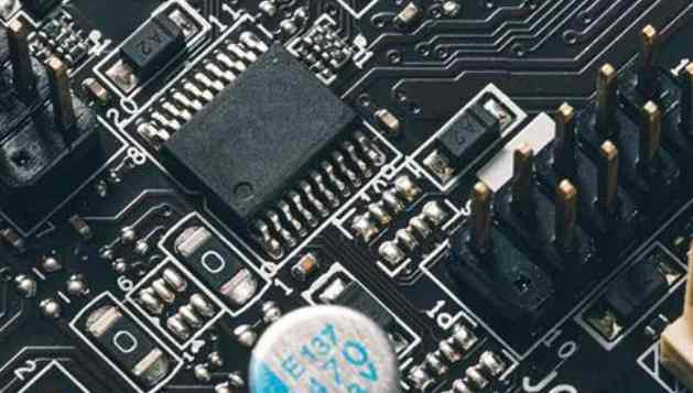
Autonomous driving and new energy vehicles are in a hot market, leading automobile PCB manufacturers full orders. At the same time, due to the strict audit of the automobile industry chain and higher requirements on stability, the gross profit rate of automotive electronics is higher than that of consumer electronics, which drives the profit of automobile and PCB manufacturers to improve.
NEPCON West China 2016 will be held in Chengdu Century City New International Convention and Exhibition Center from June 21 to 23, 2016 in order to understand the current development environment of PCB industry, help PCB manufacturers and equipment manufacturers adapt to the development trend of the industry, enhance the competitiveness of enterprises, and promote industrial upgrading. The new PCB exhibition area will undoubtedly become a professional event for PCB exhibitors and visitors.
Automatic driving and new energy vehicles promote the consumption of PCB in automobiles to increase significantly
With the gradual transition of traditional vehicles to autonomous driving through ADAS and the promotion of new energy vehicles, the penetration rate of automotive electronics is constantly increasing, and the use of vehicle PCB is becoming more and more widespread. IT is expected that in the future, with the maturity and popularization of technology, automobile IT level is improved, various functions are more and more rich and practical, and from high-end to low-end penetration.
Millimeter-wave radar brings great demand for high frequency PCB of automobile
At present, automotive millimeter wave radar is in rapid development. It is expected that the average number of millimeter wave radar used by bicycles will continue to grow in the future, and the demand for automotive radar PCB will also grow rapidly. And radar high frequency circuit to PCB board and manufacturing technology have higher requirements. Therefore, automotive radar PCB will bring higher value volume.
New energy vehicle power battery BMS
As one of the BMS hardware foundation of PCB components, its industry development will also benefit. At present, the PCB used area of luxury cars and bicycles is about 2-3 square meters. We conservatively assume that the PCB used by new energy vehicles and bicycles is 2 square meters, and calculated at 2000 yuan per square meter, the global PCB market size of new energy vehicles will reach 16.4 billion yuan in 2020.
Automotive PCB entry threshold is high, leading manufacturers have a huge first-mover advantage
Due to the special working environment, safety and high current requirements of automobile, its requirements on the reliability of PCB, environmental adaptability and other requirements are very strict. According to the introduction of Huang Weijin, chairman of Jingpeng Industry, "zero defect rate" is the basic requirement of international big factories for suppliers, which also determines whether it can enter the field of automotive PCB. Due to the high entry threshold for automotive PCBS, auto manufacturers generally do not change certified suppliers at will. Therefore, once the manufacturer can successfully enter the supply chain of the international big factory, it will not only bring the company long-term stable orders, but also bring the relatively expanded growth space for the company's operation due to the high threshold industrial characteristics. Therefore, the first-mover advantage of leading enterprises is very obvious.
At present, the western region of China follows the trend of domestic PCB industry integration, and vigorously accepts industrial transfer gathering places. In terms of land concessions, tax incentives, free recruitment and other aspects, the enterprises in the east have a great attraction, and the "flowering" momentum of PCB industry in the west appears. At the same time, with the electronic industry's demand for digital and intelligent production technology, the western region is gradually growing into the competitive high point of our manufacturing industry.

At the same time, NEPCON West China2016 will also gather a number of global well-known electronic manufacturing brands, presenting high-quality equipment technology and solutions in the fields of SMT surface mounting, EMA electronic manufacturing automation, IC & Components integrated circuits and components, PCB printed circuit boards, etc. The industry covers a wide range, which embodies the firm confidence of the organizers and exhibitors in the western electronics production and manufacturing market, and will be the most powerful wings to boost the take-off of the western electronics industry.
A rule for concluding printed circuit board design:
When the signal is transmitted on the printing plate, the delay time shall not be greater than the nominal delay time of the device used.
(3) Reduce the cross interference between signal lines:
At point A a step signal with rise time Tr is transmitted through lead AB to end B. The delay time of the signal on line AB is Td. At point D, due to the forward transmission of the signal at point A, the signal reflection after reaching point B and the delay of line AB, a page pulse signal of Tr width will be induced after Td time. At point C, due to the transmission and reflection of the signal on AB, a positive pulse with a width twice the delay time of the signal on AB is induced, that is, 2Td. This is the intersection * interference between signals. The intensity of interference signal is related to the di/at of point C signal and the distance between lines. When the two signal lines are not very long, what is seen on AB is actually the superposition of two pulses.
CMOS process of microcontrol by high input impedance, high noise, noise tolerance is also high, digital circuit is superimposed 100~200mv noise does not affect its work. If line AB in the figure is an analog signal, this interference becomes intolerable. If the printed circuit board is a four-layer board, one of which is a large area of ground, or double panels, the opposite side of the signal line is a large area of ground, the interference between the signals will be smaller. The reason is that the characteristic impedance of the signal line is reduced in a large area, and the reflection of the signal at the D terminal is greatly reduced. The characteristic impedance is inversely proportional to the square of the dielectric constant of the medium between the signal line and the ground and proportional to the natural logarithm of the thickness of the medium. If line AB is an analog signal, a large area of ground must be under the line AB to avoid interference from the digital circuit signal line CD. The distance between line AB and line CD must be two to three times greater than the distance between line AB and ground. Locally shielded ground can be used to cloth the ground wire on both sides of the side lead with a hitch.


