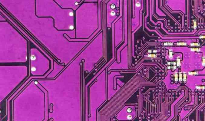
I. The design process from schematic diagram to PCB establishes component parameters - input principle netsheet - design parameter setting - manual layout - manual wiring - verification design - review -CAM output.
The spacing between adjacent wires must meet the electrical safety requirements, and in order to facilitate operation and production, the spacing should also be as wide as possible. When the wiring density is low, the distance between signal lines can be increased appropriately. For signal lines with a wide gap between high and low levels, the distance should be shortened and increased as far as possible. In general, the distance between lines should be set at 8mil.
The distance between the inner hole edge of the welding disc and the PCB edgeshould be greater than 1mm, so as to avoid defects of the welding disc during processing. When the wire connection with the pad is fine, the connection between the pad and the wire should be designed into a droplet shape. The advantage of this is that the pad is not easy to peel, but the wire and the pad are not easy to disconnect.
Practice has proved that even if the circuit schematic design is correct and the printed circuit board is improperly designed, the reliability of electronic equipment will be adversely affected. For example, if two thin parallel PCB lines are close together, there will be a delay in the signal waveform, resulting in reflected noise at the end of the transmission line. Due to the interference caused by the inconsiderate power supply and ground wire, the performance of the product will decline, therefore, in the design of printed circuit board, should pay attention to the correct method.
Four, wiring switch power supply contains high frequency signals, any printed line on the PCB can play the role of antenna, printed line length and width will affect its impedance and reactance, thus affecting the frequency response. Even printed lines that pass through the DC signal can couple from neighboring printed lines to the RF signal and cause circuit problems (or even re-radiate interference signals).
After the wiring design is completed, it is necessary to carefully check whether the wiring design conforms to the rules formulated by the designer, and also confirm whether the rules formulated meet the requirements of the PCB production process. Generally, it is necessary to check whether the distance between wire and wire, wire and component pad, wire and through hole, component pad and through hole, through hole and through hole is reasonable. Whether production requirements are met. Is the width of the power cord and ground wire appropriate? Is there any place in the PCB where the ground wire can be widened? Note: Some errors can be ignored. For example, some connectors have part of their Outline lying outside the frame, and errors occur when checking spacing. In addition, after each modification of the line and hole, it is necessary to re-cover the copper once.
What are the technical terms for each layer of PCB?
The design of printed PCB circuit boards starts from determining the size of the board. The size of printed PCB circuit boards is limited by the size of the case shell, so as to fit into the shell. Secondly, the connection mode of printed PCB circuit boards and external components (mainly potentiometers, jacks or other printed PCB circuit boards) should be considered. Printed PCB circuit boards and external components are generally connected through plastic wires or metal isolation wires. But sometimes it's designed as a socket. That is, to install a plug-in printed PCB board in the equipment, leave a contact position to act as a jack.

The following Shenzhen pcb circuit board manufacturers to introduce the various layers of PCB circuit board terminology:
Borehole layer: Borehole layer provides information about borehole during circuit board manufacturing (e.g., welding pad, which requires borehole).
Signal layer: The signal layer is used to lay out the wires on the circuit board.
Solder shield: A coating, such as solder shield paint, is applied to areas other than the pad to prevent tin from forming on these areas. The solder shield is used to match the pad during the design process and is automatically generated.
Solder paste protection layer, S-MD patch layer: it is similar to the role of the solder shield, the difference is that the corresponding surface paste type components in the machine welding pad.
Forbidden Wiring layer: Used to define the area on the board where components and wiring can be effectively placed. Draw a closed area in this layer as the wiring effective area, outside the area is not automatic layout and wiring.
Screen printing layer: Screen printing layer is mainly used to place printed information, such as the outline and annotation of components, various annotation characters, etc. Generally, all kinds of annotation characters are in the top screen printing layer, the bottom screen printing layer can be closed.
Internal power/ground layer: This type of layer is used for multilayer only, mainly for laying out power and ground wires. We call double layer, four layer, six layer, generally referring to the number of signal layer and internal power/connection layer.
Mechanical layer: It is used to set the board's dimensions, data marks, alignment marks, assembly instructions, and other mechanical information. This information varies depending on the requirements of the design company or PCB manufacturer. In addition, the mechanical layer can be attached to other layers together with the output display.
Multilayer: the solder pad on the circuit board and ChuangTou type through the hole to ChuangTou the whole circuit board, and different conductive graphic layer to establish electrical connection relationship, so the system specially set up an abstract layer - multilayer. Generally, the pad and the hole should be set on the multilayer, if the layer is closed, the pad and the hole can not be displayed.


