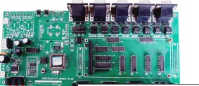
With the development of the electronics industry, the demand for printed boards is getting higher and higher. Printed board design of high density, thin wire, small aperture trend faster and faster, printed board production process is becoming more and more perfect. In this case, it is difficult to imagine that high-quality printed circuit boards can be produced without high-quality photographic substrates. Modern printed board production requires the photographic plate to meet the following conditions:

What are the conditions for the production of the camera base plate? The following Xiaobian will explain to you:
The dimensional accuracy of the photographic plate must be consistent with the accuracy required for the printed board, and the deviation caused by the production process should be compensated.
The graphics of the photographic substrate should meet the design requirements and the graphic symbols should be complete.
Figure edge straight and neat, not false; The contrast between black and white is large, which meets the requirements of photosensitive process.
The material of the photographic substrate should have good dimensional stability, that is, small dimensional changes due to changes in ambient temperature and humidity.
Double panel and multi-layer plate of the photographic base plate, requires the welding pad and the common graphics of good coincidence accuracy.
The layers of the photographic substrate should be clearly marked or named.
The photographic substrate can pass through the required light wave wavelength, and the wavelength range required for general sensitivity is 3000-4000A.
Analysis of static electricity in the process of circuit board patch processing
In the process of processing and production of electronic components, electrostatic discharge often damages the components, and sometimes even makes the components fail, resulting in serious losses, so the electrostatic protection in the processing and production of SMT patches is particularly important. Devices that are sensitive to electrostatic reactions are called electrostatic sensitive components (SSDS). Electrostatic sensitive devices mainly refer to very large scale integrated circuits, especially metallized film semiconductors (MOS circuits).
How does the static power generated during the production and processing of electronic components come from? In fact, the activities of the human body, friction, contact and separation between people and clothes, shoes, socks and other objects generated static electricity is one of the main static power sources in the production and processing of electronic components. The static electricity of the human body is the main reason for the hard (soft) breakdown of the device. The electrostatic voltage generated by human activities is about 0.5KV-2KV. In addition, the air humidity has a great impact on the electrostatic voltage, if it is in a dry environment, it will rise by 1 order of magnitude. After the human body is charged and touches the ground wire, it will produce a discharge phenomenon, and the human body will produce different degrees of electric shock response, and the degree of response is called electric shock sensitivity.
The generation of static electricity will bring no small harm to the production and processing of SMT components. Static electricity is actually a special kind of electric energy, which usually exists on the surface of the object, and is the result of the loss of balance of positive and negative charges in a local range, which is formed by the conversion of electrons or ions. Electrostatic phenomenon is the general name of the electrical phenomenon produced during the generation and disappearance of electric charges. Such as friction electrification, human electrification and other phenomena. Prevent static electricity when processing circuit board patches.
For different reasons, in some wireless communication systems, direct conversion or homodyne architectures can replace superheterodyne architectures. In this architecture, the RF input signal is directly converted to the fundamental frequency in a single step, so that most of the gain is in the fundamental frequency, and the LO is the same frequency as the input signal. In this case, the influence of a small number of couplings must be understood, and a detailed model of the "stray signal path" must be established, such as coupling through the substrate, coupling between the package pin and the bondwire, and coupling through the power cord.
Rf circuit simulation of adjacent channel interference
Distortion also plays an important role in the transmitter. The nonlinearity of the transmitter in the output circuit may cause the bandwidth of the transmitted signal to be spread over adjacent channels. This phenomenon is called "spectral regrowth". The bandwidth of the signal is limited before it reaches the transmitter's power amplifier (PA); But "cross-modulation distortion" within PA causes the bandwidth to increase again. If the bandwidth is increased too much, the transmitter will not be able to meet the power requirements of its adjacent channels. When transmitting a digitally modulated signal, it is virtually impossible to use SPICE to predict the regrowth of the spectrum. Because the transmission of approximately 1000 digital symbols must be simulated to obtain a representative spectrum, combined with a high frequency carrier, these would make transient analysis of SPICE impractical.


