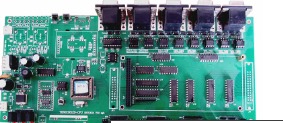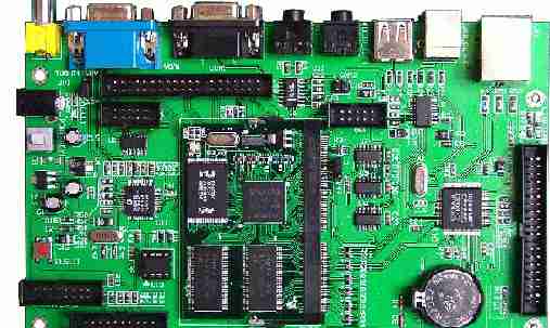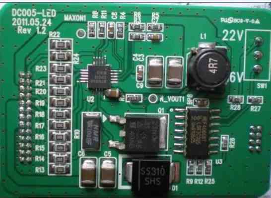
Surface Mount Technology is an electronic component assembly technology that welds electronic components (such as resistors, capacitors, integrated circuits, etc.) directly onto the surface of the printed circuit board (PCB) without the need to insert holes through pins (such as traditional THD technology). SMT patch processing conforms to the trend of The Times, to achieve non-porous patch, to achieve the miniaturization of electronic products, in the PCBA processing plant, the important characteristics of SMT patch processing are precision, speed and adaptability.
The importance of SMT for miniaturization of electronic products
1. Increase the density of the circuit board: Traditional THD technology requires a large number of holes in the PCB to insert electronic components, thus limiting the density of the board. The SMT technology can paste electronic components directly on the PCB surface, thereby reducing the spacing between components and improving the density of the circuit board.
2. Reduce the size of the circuit board: Because SMT technology can paste electronic components directly on the surface of the PCB, the size of the circuit board can be reduced, so as to achieve miniaturization of electronic products.

3. Improve production efficiency: Traditional THD technology requires electronic components to be inserted into PCB holes one by one, and connected by manual or automated means, which is time-consuming and laborious. The SMT technology can achieve efficient production through an automated way, thus improving production efficiency.
4. Improve reliability: Due to the better quality of SMT solder joints and more reliable connections, the failure rate of the circuit board can be greatly reduced, thus improving the reliability of electronic products.
5. Achieve more complex circuit design: Because SMT technology can increase the density of the circuit board, more complex circuit design can be achieved, thereby improving the function and performance of electronic products.
In summary, SMT technology plays an important role in miniaturization of electronic products, which can bring a lot of convenience to the design and production of electronic products by improving the density of the circuit board, reducing the size of the circuit board, improving production efficiency and reliability.
PCBA processing soldering soldering soldering reasons may include the following aspects:
1. Solder alloy performance: Solder alloy needs to have good wettability and fluidity, so that the solder liquid can wet and fill the weld during the welding process, so as to form a complete welded joint.
2. Peak height and cycle: the choice of peak height and cycle also has a great impact on welding quality. Reasonable matching of peak height and period can make the time and degree of solder liquid wetting element solder joint surface reach the best state, so as to form a good welding joint.
3. Component solder joint design: The solder joint design of the component will also affect the quality of the welded joint. Reasonable solder joint design can increase the contact area of the welded joint, improve the welding strength and stability.
4. Welding process parameters: The selection and adjustment of welding process parameters will also affect the quality of welded joints. For example, the adjustment of parameters such as welding temperature, welding speed, crest height and period can achieve the best wetting and filling effect of welded joints.
Solve the method of processing PCBA wave soldering tin
In the process of PCBA wave soldering, if there is a tin connection, corresponding measures need to be taken to deal with it, the common methods are as follows:
1. Adjust the welding process parameters: properly adjust the welding process parameters, such as welding temperature, crest height, period, etc., to reduce the wetting time and wetting degree during welding, and prevent the solder from forming a tin on the solder joint of the component.
2. Replace the solder alloy: try to replace other solder alloys with better wettability and fluidity to make the welding process more stable and reduce the possibility of tin connection.
3. Replace components: Some components themselves have poor wettability, easy to appear tin phenomenon, you can consider replacing other components with good weldability.
4. Check the surface treatment of PCB board and components: Improper surface treatment of PCB board and components can also easily lead to the occurrence of tin phenomenon, you can check whether there is oil, oxidation and other problems, timely cleaning and treatment of the surface.


