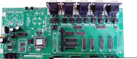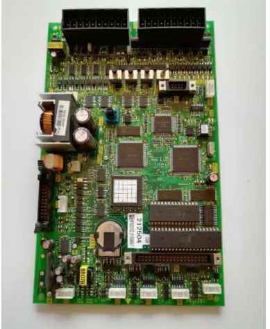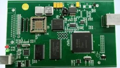
An important indicator to measure the profitability of a company or production line in SMT chip processing is: "straight-through rate." Similarly, for customers who require PCBA processing, the pass-through rate means whether the delivery date can be maximized, and the higher the pass-through rate, the shorter the delivery date. So what are the factors that affect the pass rate in SMT chip processing?

In the face of straight-through rate, we summarized two modules, one is before production and the other is after production. Today we mainly analyze the pre-production, that is, the process design stage.
The process design for pass through rate is mainly through the PCB process refinement design to ensure zero defect veneer manufacturing. Usually, we hear mostly about design for Manufacturing (DFM), and process design for pass-through rate is rarely heard because most factories don't have this knowledge, and even if they do, they don't realize the importance and complexity of pass-through rate design.
First, the process design of pass rate requires the support of experienced engineers. Process design for pass-through rate usually needs to be achieved through the following stages:
(1) Mastered a large number of typical cases.
(2) Understand the process characteristics of each package - what problems are easy to produce.
(3) Understand the mechanism and cause of each adverse phenomenon.
(4) Master effective solutions and measures.
Second, if the SMT factory has not gone through these processes, it is difficult to achieve the process design for the pass-through rate! In the production stage, there are five main process means to improve the straight-through rate, which can be improved:
(1) Optimize the design of steel mesh.
(2) Select the appropriate solder paste.
(3) Optimize the printing operation.
(4) Optimize the temperature curve.
(5) Adopt tooling to improve the process method.
kingford Electronics is a professional PCBA OEM manufacturer, providing one-stop services from upstream electronic component procurement to PCB production and processing, SMT patches, DIP plug-ins, PCBA testing, finished product assembly, etc.
The main characteristics of SMT patch processing
1, high density: Because the number of pins processed by the SMT patch is as high as hundreds or even thousands of pins, and the center distance of the pins can reach 0.3mm, the high progress BGA on the circuit board requires fine lines and fine spacing. The line width has been reduced from 0.2~0.3mm to 0.1mm or even 0.05mm, and the double lines between the 2.54mm grid have developed to 4, 5 or even 6 wires. Thin lines and fine spacing greatly increase the assembly density of SMT. In the case of high accuracy of the corresponding SMT patch processing equipment, the corresponding patch processing plant can be completed.
2, small aperture: most of the metallized holes in SMT are not used to insert component pins, and are no longer welded in the metallized holes, and the metallized holes are only used as an electrical interconnection between layers, so the aperture should be reduced as much as possible to provide more space for the SMT patch. The aperture has changed from 0.5mm in the past to 0.2mm, 0.1mm and even 0.05mm.
3, low coefficient of thermal expansion: any material will expand after heating. Polymer materials are usually higher than inorganic materials. When the expansion stress exceeds the bearing limit of the material, the material will be damaged. Because the SMT pins are too many and short, the CTE between the device body and the SMT is inconsistent, and the device damage caused by thermal stress often occurs. Therefore, the CTE of the SMT board substrate should be as low as possible to accommodate the match with the device.
4, high temperature performance is good: most of today's SMT circuit boards need to install components on both sides. Therefore, the PCB machined by SMT needs to be able to withstand two reflow soldering temperatures. At present, lead-free welding is widely used, and the welding temperature is high. After welding, the SMT chip circuit board is required to have small deformation, no foaming, the welding pad still has good weldability, and the surface of the SMT chip circuit board still has a high flatness.


