

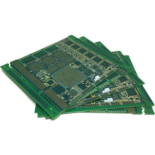
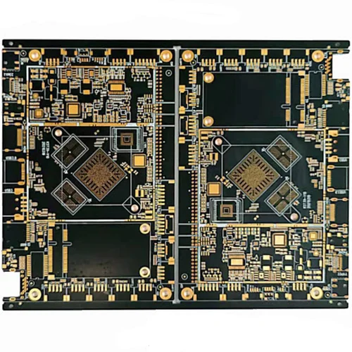
Multilayer Printed Circuit Board(PCB) Fabrication
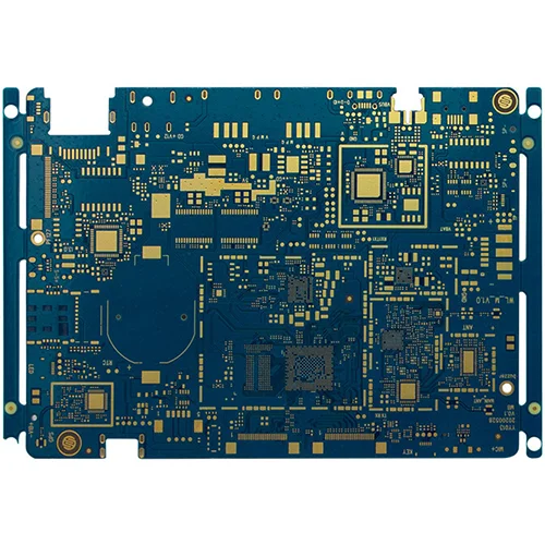
Name: Multilayer PCB
Material: KB6061, S1141, S1000, IT180
Layer: 4Layer - 48Layer Multilayer PCB
Solder Mask Color: Green/White/Blue/Red
Silk Screen Color: White/Black
Finished Thickness: 0.3mm - 6.0mm
Copper Thickness: 0.5-6OZ
Surface Treatment: Immersion Gold/OSP/HASL
Min Trace: 3mil(0.75mm)
Min Space: 3mil(0.75mm)
Application: Consumer electronics
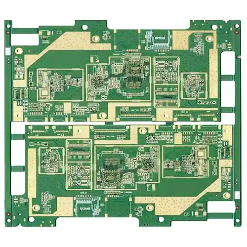
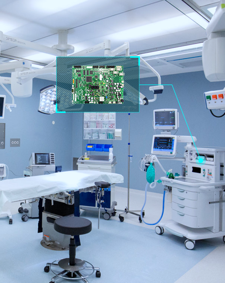
Name: Medical device PCB
Substrate: FR4
Laminate: 8L
Dielectric constant: 4.2
Plate thickness: 1.6MM
Outer copper foil thickness: 1oz
Inner copper foil thickness: 1oz
Minimum aperture: 0.2mm
Minimum line width: 0.1MM
Minimum line spacing: 0.1MM
Gold Thickness: 1U"
Application field: medical PCB
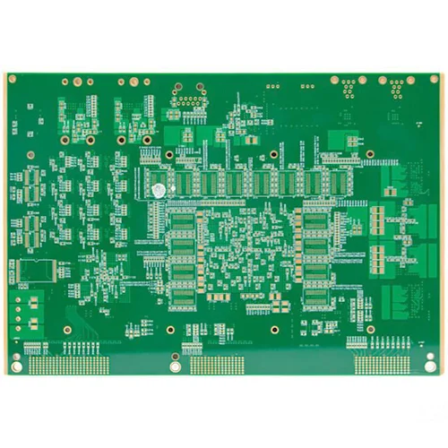
Name: Medical Equipment PCB
Substrate: FR4 Shengyi
Laminate: 6L
Dielectric constant: 4.2
Plate thickness: 1.6MM
Outer copper foil thickness: 1oz
Inner copper foil thickness: 1oz
Minimum aperture: 0.2mm
Minimum line width: 0.1MM
Minimum line spacing: 0.1MM
Gold Thickness: 1U"
Impedance requirements: L1, L3, 100 ohms
Name: 10-layer PCB circuit board
Layers: 10L
Sheet: FR4 Tg170
Plate thickness: 2.4mm
Panel size: 120*95mm/1
Outer copper thickness: 35μm
Inner layer copper thickness: 35μm
Minimum through hole: 0.20mm
Minimum BGA: 0.25mm
Line width line spacing: 3/3.2mil
Surface treatment: Immersion gold 2U''
Application field: network communication PCB board
Name: 14-layer PCB circuit board
Layers: 14L
Sheet: FR4 Tg180
Plate thickness: 2.4mm
Panel size: 120*95mm/1
Outer copper thickness: 35μm
Inner layer copper thickness: 35μm
Minimum through hole: 0.20mm
Minimum BGA: 0.25mm
Line width line spacing: 3/3.2mil
Surface treatment: Immersion gold 2U''
Application field: automotive core PCB board
Name: 12-layer PCB circuit board
Layers: 12L
Sheet: FR4 Tg150
Plate thickness: 1.2mm
Panel size: 114*96mm/2
Outer copper thickness: 35μm
Inner layer copper thickness: 35μm
Minimum through hole: 0.20mm
Minimum BGA: 0.35mm
Line width line spacing: 3.8/3.8mil
Surface treatment: Immersion gold 2U''
Application field: RK3399 development board
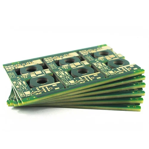
Name:Power Module PWB
Material : High TG FR4
Layer : 12Layers
Color : Green/White
Finished Thickness : 1.0mm
Copper Thickness : 2-3OZ
Surface Treatment : Immersion Gold
Min Trace : 8mil(0.2mm)
Min Space : 8mil(0.4mm)
Application : Power Module PWB
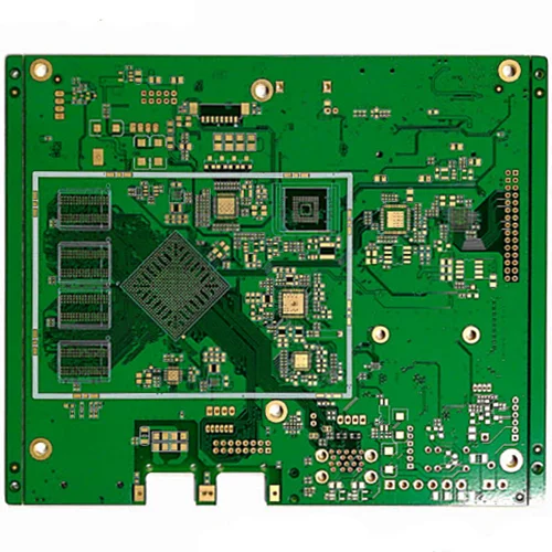
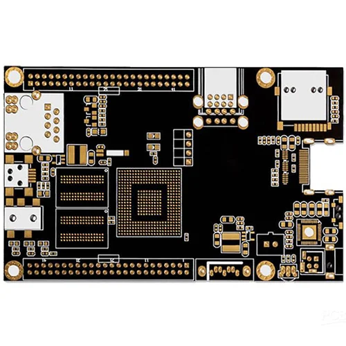
Name: 8-layer PCB circuit board
Layers: 8L
Sheet: FR4 Tg150
Plate thickness: 1.6mm
Panel size: 145*119mm/1
Outer copper thickness: 35μm
Inner layer copper thickness: 35μm
Minimum through hole: 0.20mm
Minimum BGA: 0.35mm
Line width line spacing: 3.8/3.2mil
Surface treatment: Immersion gold 2U''
Application field: face recognition PCB
6-layer industrial control PCB motherboard
Name: 6-layer industrial control PCB motherboard
Layers: 6L
Sheet: FR4 Tg150
Plate thickness: 1.6mm
Panel size: 190*150mm/2
Outer copper thickness: 35μm
Inner layer copper thickness: 35μm
Minimum through hole: 0.20mm
Minimum BGA: 0.35mm
Line width line spacing: 3/3mil
Surface treatment: Immersion gold 2U''
Application field: industrial control
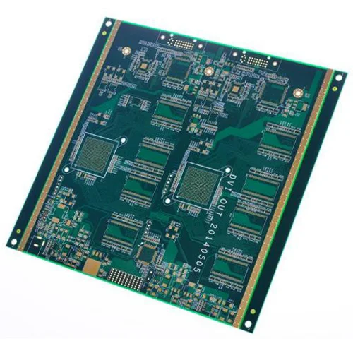
24-layer high-density high-speed PCB
Name: 24-layer high-density high-speed PCB
Material: TU872SLK
Layers: 24 layers
Thickness: 3.2±0.32mm
Minimum diameter mechanical hole: 0.25mm
Minimum track/spacing: 75/75um
Minimum plate thickness and hole ratio: 12.8:1
Surface treatment: Immersion Gold (ENIG) 0.05um
Application field: aerospace
- PCB Manufacturing Equipment
- Multilayer PCB Capability

PCB Drilling machine

PCB pattern plating line

PCB solder mask expose machine

PCB pattern expose machine

Strip film etching line

Solder mask screen silk print machine

Solder mask scrubbing line
")
PCB Flying Probe Test (FPT)

Fully automatic exposure machine
| Multilayer PCB Production Capability | |
| Item | Capability |
| Layer Count | 1-40layers |
| Base Material | KB、Shengyi、ShengyiSF305、FR408、FR408HR、IS410、FR406、GETEK、370HR、IT180A、Rogers4350B、Rogers4000、PTFE Laminates(Rogers series、Taconic series、Arlon series、Nelco series)、Rogers/Taconic/Arlon/Nelco laminate with FR-4 material(including partial Ro4350B hybrid laminating with FR-4) |
| Board Type | Backplane、HDI、High multi-layer 、blind&buried PCB、Embedded Capacitance、Embedded resistance board 、Heavy copper power PCB、Backdrill. |
| Board Thickness | 0.2-5.0mm |
| Copper Thickness | Min. 1/2 OZ, Max. 10 OZ |
| PTH Wall | 25um(1mil) |
| Maximum Board Size | 1100*500mm(43”*19”) |
| Min laser drilling size | 4mil |
| Min. Spacing/Tracing | 2.7mil/2.7mil |
| Solder Mask | Green, Black, Blue, Red, White, Yellow, Purple matte/glossy |
| Surface Treatment | Flash gold(electroplated gold)、ENIG、Hard gold、Flash gold、HASL Lead-free 、OSP、ENEPIG、Soft gold、Immersion silver、Immersion Tin、ENIG+OSP, ENIG+Gold finger, Flash gold(electroplated gold)+Gold finger, Immersion silver+Gold finger, Immersion Tin+Gold finger. |
| Min. Annular Ring | 3mil |
| Aspect ratio | 10:1(HASL Lead-free 、HASL Lead、ENIG、Immersion Tin、Immersion silver、ENEPIG);8:1(OSP) |
| Impedance control | ±5ohm(<50ohm), ±10%(≥50ohm) |
| Other Techniques | Blind/Buried Via |
| Gold Fingers | |
| Press Fit | |
| Via in Pad | |
| Electrical Test | |

High-standard confidentiality measures, signing confidentiality agreements, and all documents exporting must be approved to ensure that 100% of documents are not leaked.

we provide 24-hour service and support, you will receive a reply to your question within 2 hours and a quotation within 24 hours.

We can provide you with high frequency, high TG, high CTI, buried blind via, aluminum based PCB manufacturing, the quality is fully compliant with IPC 610-D standard, testing and quality assurance

With more than 20 years of industry experience, technology and production capacity are constantly increasing, and we can provide one-stop services from standard PCB to HDI PCB, high frequency and high...

Kingford has stable material suppliers with ten years of cooperation, such as Shengyi Technology, ITEQ, ROGERS, AGC, DUPONT, Doosan, Mitsubishi, etc.
We are a professional PCBA one-stop assembly factory, Kingford supports Multilayer PCB business, wel...
We are a professional PCBA one-stop assembly factory, Kingford supports Medical device PCB business,...
Kingford provides Medical Equipment PCB services. This is a PCBA one-stop assembly factory with seni...
We are a professional PCBA one-stop assembly factory, Kingford supports 10-layer PCB circuit board b...
We support 14-layer PCB circuit board business,Kingford is a professional one-stop PCBA service fact...
Kingford supports 12-layer PCB circuit board business, we are a professional PCBA one-stop assembly ...

We can provide the highest precision boards with up to 2 to 64 layers.
Yes, we offer multilayer PCB manufacturing with dense and high count multilayer boards.
Multilayer PCB manufacturing or production is the process of manufacturing a PCB with more than two layers combined; the characteristics of a multilayer PCB may require a more complex design than a double-sided PCB!


Telegram