Smt processing assembly line production and Smt processing
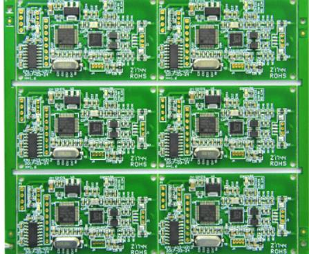
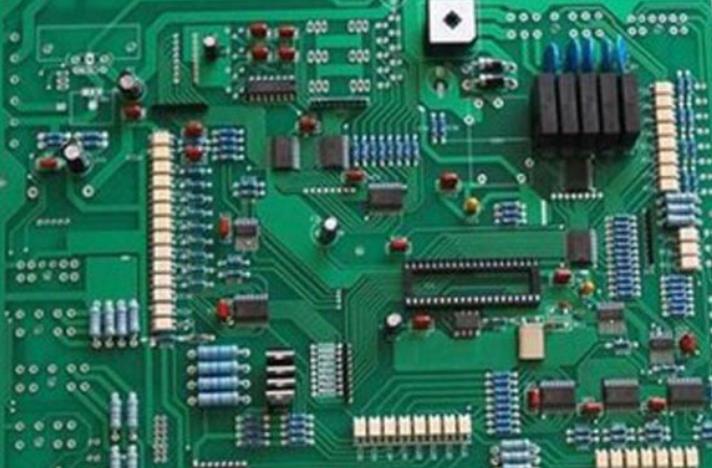
In this era, most original equipment manufacturers (OEM) and electronic contract manufacturers have to use automated equipment to Solder electronic components to printed circuit boards In addition, the equipment used for machining SMT components is completely different from the equipment used for machining through hole components According to the output, the company has one or more SMT ING production lines A typical SMT production line has the following configurations: automatic mold printer, multi area automatic chip mounter and reflow furnace
Surface mounting process
Printing is a surface mount process, which uses an automatic template printer to smear solder paste on exposed PCB pads The mechanical fixture in the printer fixes the PCB and SMT mold together. Using the printer's vision system, the bonding pad on the PCB is completely aligned with the hole on the template The thickness of the template, the size of the hole, the pressure and speed of the scraper control the amount of solder paste deposited on the SMT pad on the PCB
smt patch
Installation is the second step of SMT. Use the automatic "pick and place" machine to place SMT components on PCB. On this machine, the robot will automatically place the components on the PCB. Before that, the machine needs to be programmed using design files (Gerber files, BOM and CAD files, also known as XY data). The CAD file contains the position and rotation information of all components on the BOM.
Reflow soldering is the third step in the smt placement process, and PCB is sent to the reflow furnace. The solder paste is used as an adhesive to hold the component in place during the heating process. The oven is programmed using the thermal profile corresponding to the solder paste used. Once the solder paste reaches the reflow temperature, it will melt. In the case of double-sided boards, each side must be completed separately. Only by strictly following all specified procedures can the quality of PCBA processing be guaranteed.
How to select 3 kinds of anti painting and PCB packaging Smt processing
Circuit board

Features of PCB packaging:
PCB packaging
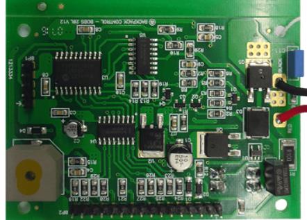
Glue is mainly used to pack the circuit board in a box with epoxy resin, which can provide a high level of protection for the circuit board. The large amount of resin around the entire unit ensures this high level of protection. This is obviously a higher level of protection than spraying 3 anti paint. In fact, potting and conformal coating provide related protection. However, potting and conformal coatings need to be tested in a variety of environments to determine their specifications and suitability. These tests usually involve exposure to controlled atmospheric conditions for a period of time.
Features of the three paint resistant coatings:
3 Anti painting
In addition to potting, it can also be coated with 3 anti paint to protect the circuit board. This is achieved by using thin films to isolate external oxidation and moisture. Since the three layers of anti paint are sprayed according to the contour of the circuit board, this will not cause any dimensional change or significant weight increase. This is actually a major advantage in favor of conformal coatings, because it is easy to make equipment portable.
The difference lies in the protection of the product and the impact on the weight and volume of the product. The specific methods to be selected need to be evaluated according to the application scenario and use environment.
The above is the explanation given by the editor of pcb circuit board company.
If you want to know more about PCBA, you can go to our company's home page to learn about it.
In addition, our company also sells various circuit boards,
High frequency circuit board and SMT chip are waiting for your presence again.


