Building 6, Zone 3, Yuekang Road,Bao'an District, Shenzhen, China
+86-13923401642Mon.-Sat.08:00-20:00
Size and weight of SMT backplane and use of glue
Requirements for Backplane Size and Weight in SMT Chip Processing
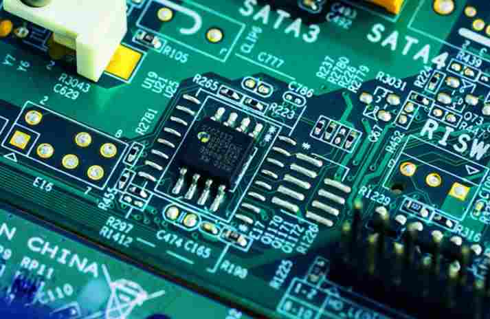
The backplane is SMT chip processing The design parameters of the backplane are very different from most other PCB design parameters Future backplanes are larger and more complex, and require unprecedented high clock frequency and bandwidth range
The user's demand for increasingly complex large size backplanes that can work with unprecedented high bandwidth is increasing, which leads to the demand for equipment processing capacity exceeding the traditional processing capacity PCB production line In particular, the backplane is larger, heavier, thicker, and requires more layers and perforations than standard PCBs
The size and weight of the backplane in SMT wafer processing need a transmission system. In general, the biggest difference between PCB and backplane lies in the size and weight of the circuit board and the handling of large and heavy raw material substrates. The standard size of PCB manufacturing equipment is usually 2.4x24 inches. However, users, especially those from special groups, need larger backplanes. This has promoted the approval and purchase of large plate conveying tools.
 At the same time, developers and designers must add additional copper layers to solve the wiring problem of connectors with large number of pins. In this way, the number of backplane layers can be added to meet customer requirements At the same time, harsh electromagnetic compatibility and impedance conditions also require additional design layers to ensure adequate shielding and improve signal integrity
With the increasing requirements of user applications on the number of circuit board layers, the alignment between layers becomes very important Tolerance convergence is required for inter layer alignment In the SMT chip processing, the size of the circuit board has been changed, and this fusion requirement has reached an unprecedented height All layout processes need to be carried out in a specific temperature and humidity controlled environment Since users need to lay more and more circuits in smaller areas in PCB wiring, in order to keep the fixed cost of the board unchanged, the size of etched copper plates is required to be smaller, which requires better alignment of copper plates between layers
Glue usage requirements during SMT chip processing
The placement and insertion hybrid assembly process of lead through hole insertion (THT) and surface mount (SMT) is the most commonly used assembly method in electronic product production. Throughout the production process, one side of the printed circuit board (PCB) assembly is bonded and cured at the beginning, and then wave soldering is performed at the end. During this period, the interval is long, and there are many other processes, and the curing of components is particularly important. This has certain requirements for the selection and use of SMT chip processing adhesive.
1. Selection of glue for SMT chip processing:
The glue used in wafer processing is mainly used in the wave soldering process of wafer modules, SOTs, SOICs and other surface mount devices. The purpose of fixing surface mount components on PCB with glue is to prevent components from falling off or shifting under the impact of high temperature wave peak. Generally, epoxy resin heat curing adhesive is used in production instead of acrylic adhesive (UV radiation is required to cure).
2. The use of glue requires SMT patch treatment:
1. The glue shall be thixotropic;
2. No drawings;
3. High wet strength;
4. No bubble;
5. Low curing temperature and short curing time of glue;
6. Have sufficient curing strength;
7. Low hygroscopicity;
8. Have good maintenance characteristics;
9. Non toxic;
10. The color is easy to identify, which is convenient to check the quality of glue point;
11. Packaging. The packaging type shall be convenient for the use of the equipment.
Requirements for Backplane Size and Weight in SMT Chip Processing
The backplane is SMT chip processing The design parameters of the backplane are very different from most other PCB design parameters Future backplanes are larger and more complex, and require unprecedented high clock frequency and bandwidth range
The user's demand for increasingly complex large size backplanes that can work with unprecedented high bandwidth is increasing, which leads to the demand for equipment processing capacity exceeding the traditional processing capacity PCB production line In particular, the backplane is larger, heavier, thicker, and requires more layers and perforations than standard PCBs
The size and weight of the backplane in SMT wafer processing need a transmission system. In general, the biggest difference between PCB and backplane lies in the size and weight of the circuit board and the handling of large and heavy raw material substrates. The standard size of PCB manufacturing equipment is usually 2.4x24 inches. However, users, especially those from special groups, need larger backplanes. This has promoted the approval and purchase of large plate conveying tools.
 At the same time, developers and designers must add additional copper layers to solve the wiring problem of connectors with large number of pins. In this way, the number of backplane layers can be added to meet customer requirements At the same time, harsh electromagnetic compatibility and impedance conditions also require additional design layers to ensure adequate shielding and improve signal integrity
With the increasing requirements of user applications on the number of circuit board layers, the alignment between layers becomes very important Tolerance convergence is required for inter layer alignment In the SMT chip processing, the size of the circuit board has been changed, and this fusion requirement has reached an unprecedented height All layout processes need to be carried out in a specific temperature and humidity controlled environment Since users need to lay more and more circuits in smaller areas in PCB wiring, in order to keep the fixed cost of the board unchanged, the size of etched copper plates is required to be smaller, which requires better alignment of copper plates between layers
Glue usage requirements during SMT chip processing
The placement and insertion hybrid assembly process of lead through hole insertion (THT) and surface mount (SMT) is the most commonly used assembly method in electronic product production. Throughout the production process, one side of the printed circuit board (PCB) assembly is bonded and cured at the beginning, and then wave soldering is performed at the end. During this period, the interval is long, and there are many other processes, and the curing of components is particularly important. This has certain requirements for the selection and use of SMT chip processing adhesive.
1. Selection of glue for SMT chip processing:
The glue used in wafer processing is mainly used in the wave soldering process of wafer modules, SOTs, SOICs and other surface mount devices. The purpose of fixing surface mount components on PCB with glue is to prevent components from falling off or shifting under the impact of high temperature wave peak. Generally, epoxy resin heat curing adhesive is used in production instead of acrylic adhesive (UV radiation is required to cure).
2. The use of glue requires SMT patch treatment:
1. The glue shall be thixotropic;
2. No drawings;
3. High wet strength;
4. No bubble;
5. Low curing temperature and short curing time of glue;
6. Have sufficient curing strength;
7. Low hygroscopicity;
8. Have good maintenance characteristics;
9. Non toxic;
10. The color is easy to identify, which is convenient to check the quality of glue point;
11. Packaging. The packaging type shall be convenient for the use of the equipment.
Just upload Gerber files, BOM files and design files, and the KINGFORD team will provide a complete quotation within 24h.


