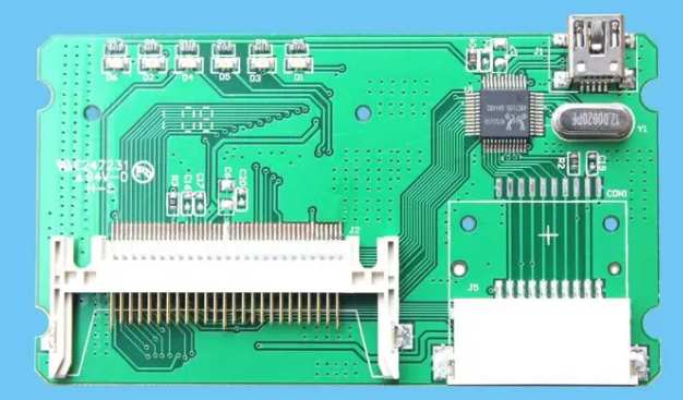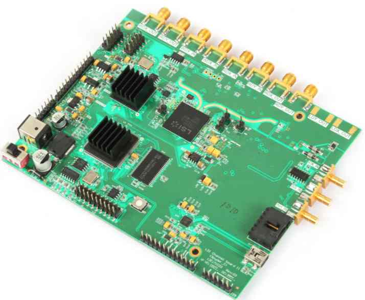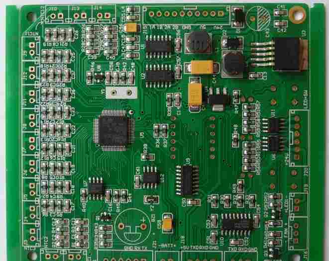
It is more efficient to do all the work in the copying software, including the placement of components support PROTEL99SE, 99SE has a very rich library of components, available for download on the Internet. This is also a key thing, PCB copy boardby hand to make components of the era has passed, because many like BGP component packaging has hundreds of elements, by hand to build components too expensive. The following patch processing manufacturer Xiaobian to explain how to choose PCB copy board software and how to improve PCB short circuit problem related knowledge.
1. How to improve the PCB short-circuit problem
PCB circuit opening and short circuit are the problems encountered by PCB manufacturers almost every day, which have been troubling the production and quality management personnel. The problems caused by it, such as replenishment due to insufficient shipment quantity, delivery delay and customer complaints, are relatively difficult to be solved by people in the industry. kingford has many years of experience in PCB manufacturing industry, mainly engaged in production management, quality management, process management and cost control. I have accumulated some experience in the improvement of PCB opening and short-circuit problems, and now I have written a summary for the discussion of PCB manufacturing in the same line, and look forward to the management of production and quality of the same line as a reference. First of all, we will summarize the main reasons for PCB open circuit into the following aspects:
1. There is scratch phenomenon before the copper clad plate enters the warehouse; 2. The copper clad plate is scratched in the process of opening; 3. The copper clad plate is scratched when drilling; 4. The copper clad plate is scratched in the transfer process; 5. When stacking plates after copper sinking, copper foil on the surface is injured due to improper operation; 6. The copper foil on the surface of the production plate is scratched when the machine is too horizontal.
Improvement method:
1. IQC must carry out spot inspection before entering the warehouse to check whether the surface of the copper clad plate is scratched and exposed to the substrate. If so, contact the supplier in time and make appropriate treatment according to the actual situation.
2. The copper clad plate is scratched in the process of opening, the main reason is that there are hard objects on the surface of the opening machine. Friction between the copper clad plate and the objects causes the copper foil scratch to form the phenomenon of exposing the substrate.
3, the copper clad plate is scratched when drilling, the main reason is that the main shaft clip is worn, or there is no debris in the clip is clean, PCB proofing grasp the drill beak is not strong, the drill beak is not on the top, slightly longer than the length of the drill beak, drilling height is not enough, the machine tool move when the drill beak tip scratch copper foil formation exposed substrate phenomenon. a. The clip can be replaced by the number of times recorded by the knife or according to the wear degree of the clip; b. Clean the clip regularly according to the operating rules to ensure that there is no debris in the clip.
4, the plate is scratched in the process of transport: a, handling personnel lift the amount of the board is too much, the weight is too large, the board is not lifted when handling, but dragged up, causing the Angle of the board and the friction of the board surface and scratched the board; b. When putting down the board, it is not put neatly. In order to rearrange the board, it is forced to push the board, causing friction between the board and the board and scratching the surface.
5, after copper sinking, the whole board plating after stacking board due to improper operation was scratched: after copper sinking, the whole board plating after storage board, because the board is stacked together, there is a certain amount of weight is not small, then put down, the Angle of the board down and with a gravitational acceleration, the formation of a strong impact impact on the board surface, resulting in scratches on the substrate. 6, the production board is scratched in the horizontal machine: a, the baffle of the grinding machine sometimes contact the surface of the plate, the edge of the baffle is generally uneven and the advantages are raised, the board surface is scratched when the plate is crossed; b, stainless steel drive shaft, due to damage into a pointed object, when the plate scratches the copper surface and exposed substrate.

2. How to choose PCB copying software
Copy board software is good or bad mainly depends on whether the function is complete, it is best to put all the work can be done in the copy board software, so high efficiency, including the placement of components support PROTEL99SE for the best, 99SE components library is very rich, can be downloaded in the Internet. This is also a key thing, PCB copy board by hand to make components of the era has passed, because many like BGP component packaging has hundreds of elements, by hand to build components too expensive. In order to be stable and reliable circuit, in the design of the circuit generally to have a large piece of copper and power or ground connection, so as to reduce the noise and interference of the circuit.
So it involves the problem of network copper, for complex circuit boards, copper is a lot of connection and a lot of isolation, so if the problem is not solved, copper can not be realized, so here must define the network to lay copper (" the same network is connected, different networks are isolated "), simply fill all the copper skin will appear short circuit. This is also a key problem to measure the software of copying board. After choosing the software with perfect functions, in order to ensure the perfect effect, we should also have rich experience and skilled skills in technology for the copy board of double layer and multilayer board. Because the holes of the same double-layer or multi-layer PCB board are in the same position, but the line connection is different, then, when the wiring rules of the original board are described in the board copying software, the PCB file of the top layer that has been copied out of the double-layer board is stacked on the scanning image of the other layer, and the holes of the two overlap, and then set the top line and screen printing are not displayed. Delineate another layer of circuit according to the location of the holes, so that the exported PCB file contains both sides of the two panels. The same with multilayer board, only need to sand off the surface after tracing the surface PCB file diagram, so that the inner line rules exposed, and then with the help of board copying software in the same technical way to copy out. At present, the most commonly used copy board software on the market is PROTEL99SE, in addition to quickpcb 2005 V3.0 and various versions of color copy board software.
Among them, Protel99SE was originally applied to Windows9X/2000/NT operating system EDA design software, using the design library management mode, can carry out networking design, has a strong ability to exchange data and open and 3D simulation function, is a 32-bit design software, can complete the circuit schematic design, Printed circuit board design and programmable logic device design and other work, can design 32 signal layers, 16 power sources - the formation and 16 machining layers. quickpcb 2005 V3.0 software all operation in line with the majority of designers operating habits, can greatly improve the efficiency of copy board, and relieve the operators of the pain of testing. Copy board one-time qualified rate can also be further guaranteed. Place pad, hole, line, arc, through hole, component, FILL, POLYGON, text; Element attribute setting, grid setting; The CTRL key automatically captures the center of the grid and elements; SHIFT Select, deselect, cut, copy, delete, rotate, mirror, and repeat; 32 layers of setting function, zoom display;


