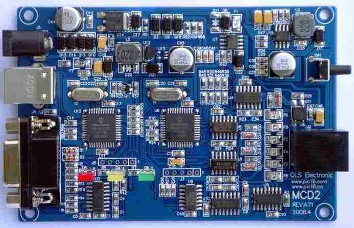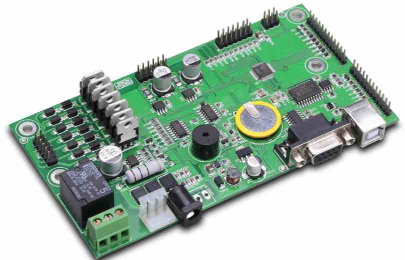
How to guarantee the quality of PCB processing? From what aspects can we correctly understand clearly some quality problems in PCB processing? We summarized the following three points, so that we can have a more comprehensive understanding of the quality monitoring of PCB processing. The following patch processing manufacturers will explain how to accept PCBA processed products and how to ensure the quality of PCB processing knowledge.
1. How to ensure the quality of PCB processing
1: pressure (patch height) - Patch pressure (height) should be appropriate
The solder end or pin of the component shall not be less than 1/2 thickness and be immersed in the solder paste. The solder paste extrusion amount (length) should be less than 0.2mm for the common element patch, and the solder paste extrusion amount (length) should be less than 0.1mm for the narrow space component patch. The patch pressure is too small, the welding end or pin of the component floats on the surface of the solder paste, the solder paste does not stick to the component, and the position is easy to move during transfer and reflow welding.
2: the components are correct -- each assembly position number is required
The type, model, nominal value and cabinet polarity of the components and other characteristic marks should conform to the assembly drawing and specification of the product, can not be pasted in the wrong position.
Three: accurate position -- the end or pin of the components and the pad figure should be aligned and centered as far as possible.
The installation location of components shall meet the technological requirements.
Because the two end Chip element self-positioning effect is relatively large, when mounting the length direction of the element two ends as long as the corresponding pad, the width direction of 1/2 lap on the pad, and then flow welding can be self-positioning, but if one of the end does not lap on the pad, then flow welding will produce displacement or suspension bridge: For SOP, SOJ, QFP, PLCC and other devices, the self-positioning effect is relatively small, and the mounting deviation cannot be corrected by reflow welding. Therefore, when mounting, it is necessary to ensure that 3/4 of the width of the pin is on the pad, and the toe and heel of the pin should also be on the pad. If the mounting position exceeds the allowable deviation range, manual correction must be carried out before entering the reflow welding furnace welding.

2. How to accept PCBA processed products
Acceptance criteria for PCBA processed products
1. The polarity point on the screen reversal element (white screen printing) is consistent with the direction of the screen printing on the PCB board. The polarity point on the (acceptable) element (white screen) is inconsistent with the PCB board diode screen. (Rejected)
2. The maximum height (E) of the solder joint with too much tin may extend to the metallized top of the PAD or end cap, extending to the weldable end, but not touching the body of the element. The solder has touched the top of the assembly body. (Rejected)
3. Reverse if exposed to the exposed electrical material, the chip component will have the opposite direction to the material surface and the printed surface. Only one component ≤0402 is allowed to be reversed per PC board. (Acceptable) If exposed electrical material is present, the chip component will have the same material surface as the printed surface. The chip assembly has two or more components, with each Pcs plate ≤0402. (Rejected)
4. The solder joint between the air welded component lead and PAD is wet and full, and the component lead is not lifted. The (acceptable) component leads are not coplanar, preventing acceptable welding. (Rejected)
5. In the reflux process of cold welding, the solder paste is completely extended, the tin on the solder joint is completely wet and the surface is smooth. The solder paste on the ball is not fully reflow, the tin is black and irregular in appearance, and the solder paste has incomplete melted tin powder. (Rejected)
6. The patch bit needs to be installed but is not installed for a few BOM items. (Rejected) BOM Request Patch number Components are not required to be installed, but components are installed, and redundant parts are found in any location. 7. Damage any edge peel less than 25% of component width (W) or component thickness (T), and top metal plating missing up to 50% (each end). (Acceptable) any cracks or dents exposed due to rattling, cracks or any damage to the body of the glass part, any resistance material gaps, any cracks or indentations. (Rejected)
8. The area of foaming, laminating foaming and laminating shall not exceed 25% of the spacing between plating through holes or internal lines. The area of foaming and delamination exceeds 25% of the spacing between the plated through holes or internal conductors, and the area of foaming and delamination reduces the spacing of conductive patterns to a minimum electrical gap. Only strict implementation of acceptance procedures can ensure the quality of PCBA processed products. Only by paying more attention to quality can we survive in the increasingly competitive market.
kingford PCBA processing advantage
▪ SMT workshop: We have imported SMT machines and several sets of optical inspection equipment, with a daily output of 4 million. Each process is equipped with QC personnel, who can keep an eye on product quality. ▪ DIP production line: We have two wave-soldering machines, among which there are more than 10 old employees who have worked for more than three years. The skilled workers can weld all kinds of plug-in materials.
2. Quality assurance, high cost performance. High-end equipment can stick precision special-shaped parts, BGA, QFN, 0201 materials. Can also template patch, loose material hand. ▪ Sample and size batch can be produced, proofing from 800 yuan, batch 0.008 yuan/point, no start-up fee.
3. Rich experience in SMT and welding of electronic products, stable delivery. Accumulated services for thousands of electronic enterprises, involving many kinds of automotive equipment and industrial control motherboard SMT processing services, products are often exported to Europe and the United States, quality can be affirmed by new and old customers. ▪ On time delivery, normal 3-5 days after complete materials, small batch can also be expedited on the same day shipment.
4. Strong maintenance ability, circuit board erfect after-sales service ▪ Experienced maintenance engineers, can repair all kinds of patch welding caused by bad products, to ensure the connection rate of each piece of . ▪ 24-hour customer service staff at any time response, the fastest speed to solve your order problems


