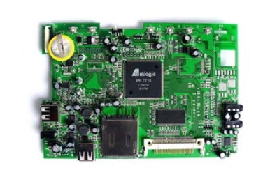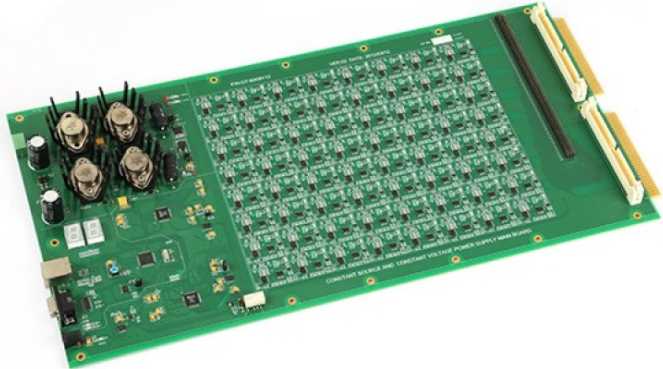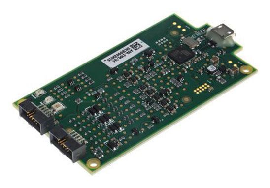
SMT basic process elements include: screen printing (or dispensing), mounting (curing), reflow soldering, cleaning, testing, repair
1. Screen printing: Its function is to leak solder paste or patch glue onto the PCB pad to prepare for the welding of components. The equipment used is screen printing machine (screen printing machine), located at the front end of the SMT line.
2, dispensing: it is to drop the glue to the fixed position of PCB, its main role is to fix the components to the PCB board. The equipment used is the dispensing machine, which is located at the front end of the SMT production line or behind the testing equipment.
3. Mounting: Its function is to accurately install the surface assembly components to the fixed position of PCB. The equipment used is the SMT machine, which is located behind the screen printing machine in the SMT production line.
4, curing: its role is to melt the patch glue, so that the surface assembly components and PCB board firmly bonded together. The equipment used is the curing furnace, which is located behind the SMT machine in the SMT line.
5, reflow welding: its role is to melt the welding paste, so that the surface assembly components and PCB board firmly bonded together. The equipment used is reflow furnace, which is located behind the SMT machine in the SMT line.
6, cleaning: its role is to assemble the PCB board above the welding residue harmful to human health, such as flux, etc., to remove. The equipment used is a cleaning machine, the position can not be fixed, can be online or not online.
7, detection: its role is to assemble the PCB board welding quality and assembly quality detection. The equipment used includes magnifying glass, microscope, online tester (ICT), flying needle tester, automatic optical testing (AOI), X-RAY testing system, function tester, etc. Location According to the need of detection, can be configured in the production line of the appropriate place.
8, repair: its role is to detect the fault of the PCB board rework. The tools used are soldering iron, repair workstation, etc. Configuration anywhere in the production line.
I. Single-side assembly:
Incoming material inspection => Silk screen welding paste (spot patch glue) => Patch => Drying (curing) => Reflux welding => Clean. Detection => repair
Two, double-sided assembly:

A: incoming material inspection => PCB side A screen printing solder paste (spot patch glue) => Patch => Drying (curing) => A-side reflow welding => Clean. Turn over a board. PCB side B screen printing solder paste (spot patch glue) => Patch => Dry => Reflow welding (preferably only for B side => Clean. Detection => Repair)
This process is suitable for PCB with PLCC and other large SMDS on both sides.
B: Incoming material inspection => PCB side A screen printing solder paste (spot patch glue) => Patch => Drying (curing) => A-side reflow welding => Clean. Turn over a board. PCB B spot adhesive patch => Patch => Cure => B side wave soldering => Clean. Detection => Repair)
This process is suitable for reflow welding on side A and wave soldering on side B of PCB. This process is recommended when only SOT or SOIC (28) pins are below in the B-side assembled SMDS of the PCB.
Iii. Single-side mixed loading process:
Incoming material inspection => PCB side A screen printing solder paste (spot patch glue) => Patch => Drying (curing) => Reflux welding => Clean. Plug-in => Wave soldering Clean. Detection => repair
Four, double-sided mixed loading process:
A: incoming material inspection => PCB B spot patch adhesive => Patch => Cure => Turn over a board. PCB side A plug-in. Wave soldering Clean. Detection => repair
Stick before insert, suitable for SMD components more than separate components
B: Incoming material inspection => PCB side A plug-in (pin bent) => Turn over a board. PCB B spot patch adhesive => Patch => Cure => Turn over a board. Wave soldering Clean. Detection => repair
Insert before paste, suitable for separated components more than SMD components
C: incoming material detection => PCB side A silk screen solder paste => Patch => Dry => Reflux welding => Plug-in, pin bent => Turn over a board. PCB B spot patch adhesive => Patch => Cure => Turn over a board. Wave soldering Clean. Detection => Reassemble side A mixed, side B pasted.
D: incoming material detection => PCB B spot patch adhesive => Patch => Cure => Turn over a board. PCB side A silk screen solder paste => Patch => A-side reflow welding => Plug-in => B side wave soldering => Clean. Detection => Reassemble side A mixed, side B pasted. First stick two sides SMD, reflow welding, after insertion, wave soldering
E: incoming material detection => PCB side B screen printing solder paste (spot patch glue) => Patch => Drying (curing) => Reflux welding => Turn over a board. PCB side A silk screen solder paste => Patch => Drying = reflow welding 1 (local welding can be used) => Plug-in => Wave crest welding 2 (if there are few plug-in components, manual welding can be used) => Clean. Detection => Reassemble side A and reassemble side B.
Five, double-sided assembly process
A: Incoming material detection,PCB side A silkscreen welding paste (spot patch glue), patch, drying (curing), side A reflow welding, cleaning, turning over; PCB side B screen printing welding paste (spot patch glue), patch, drying, reflow welding (best only for side B, cleaning, testing, repair)
This process is suitable for PCB with PLCC and other large SMDS on both sides.
B: Incoming material detection,PCB side A silkscreen welding paste (spot patch glue), patch, drying (curing), side A reflow welding, cleaning, turning over; PCB's B side patch glue, patch, curing,B side wave soldering, cleaning, testing, repair) This process is suitable for PCB's A side reflow welding,B side wave soldering. This process is recommended when only SOT or SOIC (28) pins are below in the B-side assembled SMDS of the PCB board.


