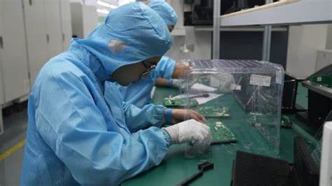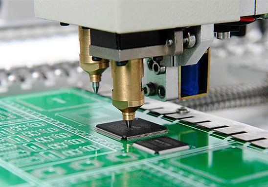
The DIP plug-in process is a part of the PCBA process after the SMT patch process. Theut need to be ma DIP plug-in refers to large-sized components that cannot be mounted by a machine, bnually plugged in, and then soldered by wave soldering, and the final product is formed. .
The DIP plug-in process can be roughly divided into plug-in, wave soldering, foot cutting, inspection, testing and other processes. The plug-in is to insert the chip-processed components into the corresponding position of the PCB board to prepare for the wave soldering; the wave soldering is to insert the plug-in. Put the PCB board into the conveyor belt of wave soldering, and complete the soldering of the PCB board after spraying flux, holding heat, wave repair welding, cooling and other links; the cutting foot is to cut the soldered PCBA board to achieve a suitable Dimensions; Test After the welding is completed, the finished PCBA board needs to be tested. If there is a defect in the function, it must be repaired and re-tested. If there is no problem in the test, it will be packaged and put into storage.

DIP plug-in process is an important link in the PCBA processing. The quality of DIP plug-in determines the quality of PCBA processing. Therefore, we need to pay attention to the following when performing DIP plug-in.
1. Before plugging in, check whether there are oil stains, paint and other unclean objects on the surface of electronic components.
2. During the plug-in process, it is necessary to ensure that the electronic components and the PCB are flat. After the plug-in is completed, the electronic components must be in a flat state.
3. If there is a direction indicator on the electronic component, it must be plugged in the correct direction, and do not plug in at will.
4. When plugging in, pay attention to the force of the plug-in. Do not use too much force when plugging in, which will cause damage to components or damage to the PCB board.
5. Do not insert the edge of the PCB board when inserting electronic components, and pay special attention to the height of electronic components and the spacing between electronic components.
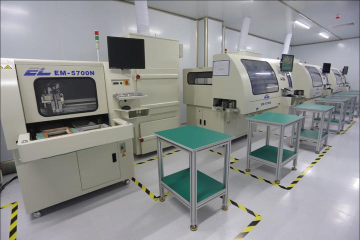
Shenzhen Kingford Technology Co., Ltd. has a factory area of 30,000 square meters and 24 SMT production line, 8 plug-in lines, 4 wave soldering lines, 8 assembly lines, 4 packaging lines, with a total investment of 1 billion, equipped with advanced and perfect digital management system, committed to building an industrial 4.0 smart factory. It has perfect industry 4.0 solutions, PCBA processing services, SMT chip processing services, OEM electronic processing services, ODM/OEM and material services.


