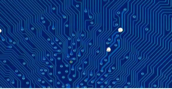
PCB circuit board with insulation board as the base material, cut into a certain size, it is accompanied by at least one conductive graphic, and cloth holes (such as component holes, fastening holes, metallization holes, etc.), used to replace the chassis of the previous device electronic components, and to achieve the mutual connection between electronic components.
Selection of the base material of PCB circuit board:
1. Sinking gold plate
The biggest problem of this kind of substrate is the problem of "BlackPad", so there are many big factories in the lead-free process do not agree to use, but most domestic manufacturers use this process.
2. Silver plate
Although the "silver" itself has a strong mobility, resulting in leakage of electricity, but today's "dipping silver" is not the past pure metal silver, but with organic matter co-plated "organic silver", so it has been able to meet the needs of the future lead-free process, its weldability life is longer than OSP plate.
3.OSP board
OSP process has the lowest cost and is easy to operate, but the popularity of this process is still poor due to the need to modify the equipment and process conditions of the assembly plant and the poor heavy industry, so the use of this kind of plate, after high temperature heating, the protective film pre-covered on the PAD is bound to be damaged, resulting in reduced solderability, especially when the substrate is more serious after secondary backwelding. Therefore, if the process needs to go through another DIP process, the DIP end will face the challenge of welding at this time.
Talking about the methods to prevent the warping of PCB circuit board
The chassis of the electronic components is installed, and the interconnection between the electronic components is realized. Then the methods to prevent the warping of PCB circuit boards are:

1. Cold press after the laminated thick stress relief plate, trim the raw edge;
2. Baking plate before drilling: 150 degrees for 4 hours;
3. Engineering design: interlayer semi-cured sheet arrangement response; Multi-layer core plate and semi-cured sheet should use the same supplier's product; The graphic area of the outer C/S plane is as close as possible, and an independent grid can be used;
4. The drying plate is generally 150 degrees for 6-10 hours before blanking, removing water vapor in the plate, further curing the resin completely, and eliminating the stress in the plate; Drying plate before opening, both inner layer and double side are needed;
5. Before laminating laminates, attention should be paid to the warp and weft direction of the curing sheet: the warp and weft contraction ratio is not the same, and the semi-curing sheet should be careful to distinguish the warp and weft direction before laminating; The core plate should also pay attention to the warp and weft direction when cutting; Generally, the direction of the plate curing sheet is meridional. The long direction of the copper-clad plate is meridional;
6. It is best not to go through mechanical grinding brush, it is recommended to use chemical washing; Special fixture is used during plating to prevent bending and folding of the plate 7 After spraying tin, it is naturally cooled to room temperature on the flat marble or steel plate or cleaned after cooling on the air float bed; Warped plate treatment: 150 degrees or hot pressing for 3--6 hours, using flat and smooth steel plate pressure, 2-3 times baking.
What are the effects of warping on components during PCB manufacturing? PCB board warping will cause inaccurate positioning of components; When the plate is bent in SMT and THT, the component pins are not integrated, which will bring a lot of difficulties to the assembly and installation work. The board on which the components are installed is bent after welding, and the component feet are difficult to cut neatly. The PCB board can not be installed in the chassis or the socket inside the machine, so preventing the PCB board warping is a very important step.
The concept and classification of the substrate in the PCB board
PCB circuit board, also known as printed circuit board, is a provider of electrical connections for electronic components. It has a history of more than 100 years; Its design is mainly layout design; The main advantage of using circuit boards is to greatly reduce wiring and assembly errors, improve the level of automation and production labor rate.
What is the substrate in a PCB board? PCB manufacturers to tell you:
Today, printed circuit boards have become an indispensable component of most electronic products. In the manufacturing of single and double-sided printed boards, hole processing, electroless copper plating, copper plating, etching and other processing are selectively carried out on the substrate material - copper coated foil laminate to obtain the required circuit graphics.
Another kind of multi-layer printed board is also based on the inner core thin coppered foil plate, and the conductive pattern layer and the semi-cured sheet are alternately bonded together by one-time lamination to form an interconnect between more than three conductive pattern layers. Therefore, it can be seen that as the substrate material in the manufacture of printed boards, whether it is copper clad foil or semi-cured sheet, it plays a very important role in printed boards. It has three functions: conduction, insulation and support. The performance, quality, processability, manufacturing cost, and manufacturing level of printed boards depend to a large extent on the substrate material.
There are many kinds of classification methods for copper-clad foil. Generally, according to the different reinforcement materials of the board, it can be divided into five categories: paper base, glass fiber cloth base, composite base (CEM series), laminated multilayer board base and special material base (ceramic, metal core base, etc.). If it is classified according to the resin adhesive used in the board, the common paper based CCI. There are: phenolic resin, epoxy resin (FE - 3), polyester resin and other types. Common glass fiber cloth CCL has epoxy resin, which is currently the most widely used type of glass fiber cloth.
Classification of substrate. General printed board substrate materials can be divided into two categories: rigid substrate materials and flexible substrate materials. An important variety of general rigid substrate materials is copper-clad plate. It is made of reinforcing material, impregnated with resin adhesive, dried, cut, laminated into billet, then coated with copper foil, using steel plate as a mold, and made by high temperature and high pressure forming processing in hot press. The general semi-cured sheet for multi-layer plates is a semi-finished product in the production process of copper clad plates (mostly glass cloth impregnated with resin and dried).


