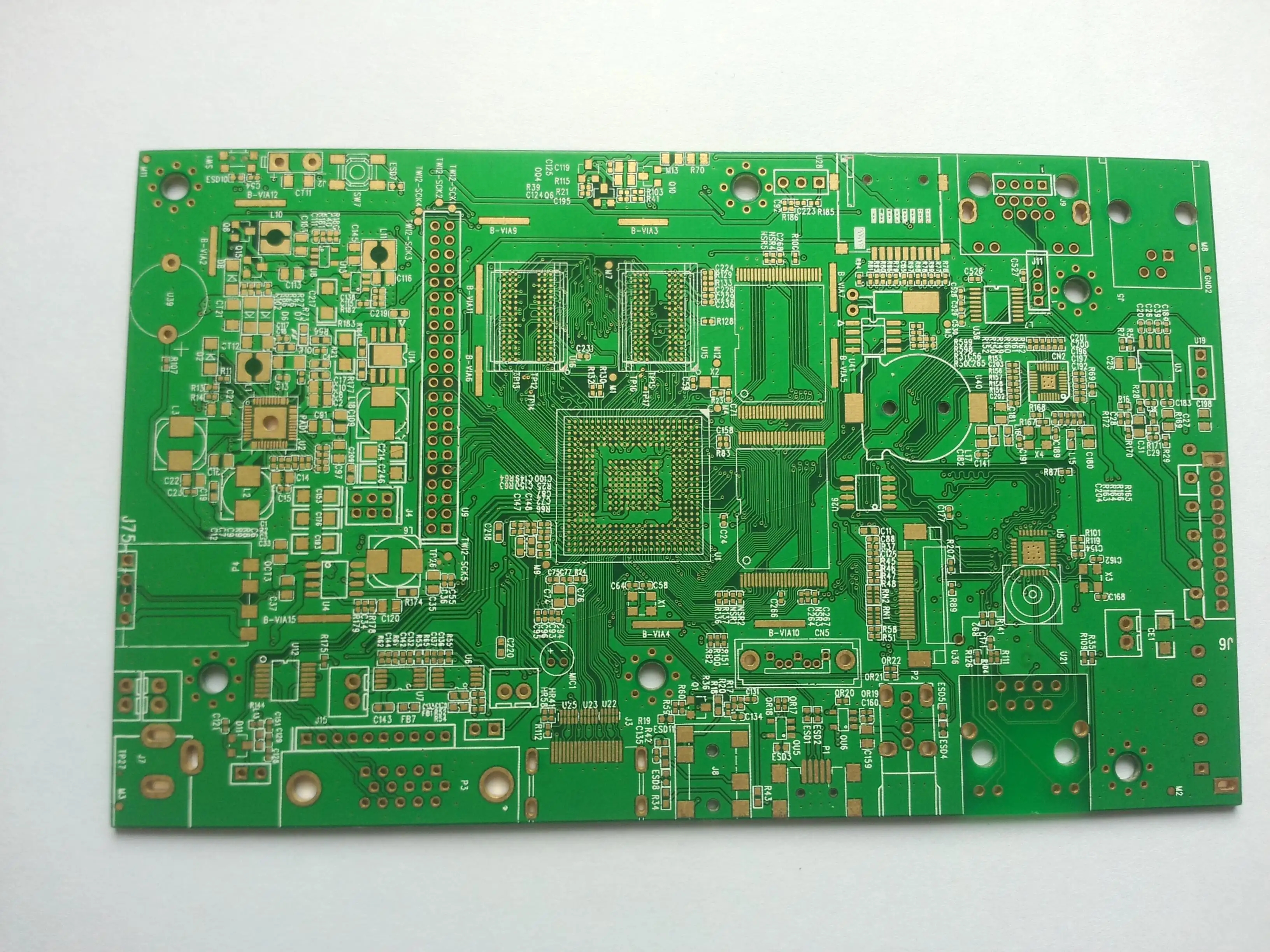
Development of Copper Foil Technology for Printed Circuit Boards
(1) PCB copper foil production
Copper foil production began in 193.7 at Anaconda copper refinery in the United States At that time, copper foil was only used for waterproofing of wooden roofs In the early 1950s, along with PCB industry, copper foil industry became an important cutting-edge industry related to electronic information industry
In 1955, Yates Company was separated from Anaconda Company and became the first company specialized in producing electrolytic copper foil for PCB circuit board in the world. In 1957, Gould Company of the United States also invested in this industry, separating Yates from the global exclusive market of copper foil for PCB multilayer circuit boards. After Mitsui introduced the American copper foil manufacturing technology in 1968, Furukawa and Nippon Mining of Japan cooperated with Yates and Gould respectively, and made great progress in the Japanese copper foil industry.

In 1972, Yates Corporation issued its electrolytic copper foil production patent (US patent 3674656), marking a new stage in the technology of electrolytic copper foil manufacturing and surface treatment.
According to statistics, the global output of electrolytic copper foil for PCB in 1999 was about 180000 tons. Among them, Japan has 50000 tons, Taiwan has 43000 tons, China has 19000 tons, and South Korea has 10000 tons. It is estimated that the global production of electrolytic copper foil will increase to 253000 tons in 2001. The fastest growth rates are Japan (73000 tons in 2001) and Taiwan (65000 tons in 2001).
Japan is the first country in copper foil production and science and technology in the world. Thanks to the development of printed circuit board and copper clad laminate, it has made rapid progress in copper foil production and science and technology in recent years. In recent years, the company has also established overseas manufacturers invested by Japan in North America, mainland China, Taiwan, Southeast Asia, Europe and other countries and regions. Major manufacturers of electrolytic copper foil in Japan include Mitsui Metal Mining Company, Japan Energy Company (formerly Japan Mining Company), Electric Company, Fukuda Metal Foil Industry Company, Japan Electrolysis Company, etc. The production characteristics of electrolytic copper foil in Japan are: in recent years, it is developing towards more advanced technology and cutting-edge products.
Taiwan is now the world's second largest producer of electrolytic copper foil. Major large-scale manufacturers include Changchun Petrochemical Company, Taiwan Copper Foil Company, South Asia Plastic Company, etc.
PCB Cooper
(2) High performance electrolytic copper foil
In recent years, the world copper foil industry has continuously innovated and developed some high-performance electrolytic copper foil manufacturing technologies One bit overseas copper foil market research experts recently concluded that due to high-density fine linearization (LIS=0.10), the market share of high-performance copper foil will reach more than 40% mm/0.10 mm), multi-layer (6 layers), thinned (0.8 mm) and high-frequency PCB multilayer circuit boards in the near future The main types and characteristics of these high-performance copper foils are as follows
Excellent tensile strength and elongation Copper foil Excellent tensile strength and elongation Electrolytic copper foil, including under normal and high temperature. Under normal conditions, increasing the tensile strength and high elongation can improve the processing efficiency of electrolytic copper foil, improve the hardness, avoid wrinkling and improve the production qualification rate. High temperature ductile copper foil and high temperature copper foil with high tensile strength can improve the thermal stability of PCB and avoid deformation and warping. At the same time, the copper foil cracks at high temperature (usually copper foil is used in the inner layer of PCB multilayer board to form a through hole inner ring, which is easy to crack when immersed in welding). The use of HTE copper foil can be improved.
2. Thin copper foil
The progress of high-density wiring technology for PCB multilayer boards makes it unsuitable to continue to use traditional electrolytic copper foil to make high-precision PCB board graphics. In this case, a new generation of electrolytic copper foil with one-to-one low profile (LP) or ultra-low profile (VLP) has emerged. In the early 1990s (1992-1994), the United States (the Arizona factory in Gould) and Japan (Mitsui Metal Corporation, Guhe Electric Corporation, and Fukuda Metal Industry Corporation) successfully developed thin copper foil almost simultaneously.
Generally speaking, the original foil is made by electroplating, and the current density used is very high. In this case, the micro crystallization of the original foil is very rough, showing a coarse columnar crystal. The "ridge line" of the transverse fault in the fault slice is highly fluctuating. The crystallization of LP copper foil is very fine (2) mm or less), which is an equiaxed grain, without columnar crystals, and crystallizes into a sheet with flat edges. The surface roughness is low. By actual measurement, the average roughness (R.) of VLP copper foil is 0.55. MM (1.40 for copper foil generally). The maximum roughness (R m? X) is 5.04mm (usually 12.50 copper foil) mm. Compare the efficiency of various types of copper foil shown in Table 5-1-8 (the data in this table are used as examples of various types of copper foil products of Mitsui Metal Co., Ltd. in Japan).
VLP and LP copper foils not only guarantee the general efficiency of ordinary copper tubes, but also have the following characteristics.
(1) The initial precipitation of VLP and LP copper foils is a crystalline layer with a certain distance. The crystallization of VLP and LP copper foil is not like vertical connection overlapping upward, but a slightly concave and convex plane plate. This crystal structure prevents sliding between metal particles and has greater resistance to deformation caused by external conditions. In this case, the tensile strength and elongation (normal and thermal) of copper foil are superior to ordinary electrolytic copper foil.
(2) LP copper foil is smoother and finer than ordinary copper foil on rough surface. In the interface between copper foil and substrate, there is no residual copper powder (copper powder transfer phenomenon) after etching, which improves the surface resistance and interlayer resistance characteristics of PCB, and improves the reliability of dielectric efficiency.
(3) It has a high thermal stability, and because of the multilayer, it will not recrystallize copper on the thin substrate.
(4) The etching time of graphic circuit is less than that of common electrolytic copper foil. Reduce side etching. The white spot is reduced after etching. Suitable for fine manufacturing.
LP copper foil has high hardness, which improves the drillability of PCB multilayer boards. It is also more suitable for laser drilling.
The surface of low-voltage copper foil is relatively flat after being pressed and formed by PCB multilayer board, which is suitable for production of precision lines.
The thickness of low-voltage copper foil is uniform, the signal transmission delay is small after the PCB circuit board is made, the characteristic impedance is well controlled, and the wireless line to line, layer to layer noise, etc.
Thin copper foil is very different from ordinary electrolytic copper foil in fine structure such as grain size, distribution, crystal orientation and distribution. In the original production of ordinary electrolytic copper foil, on the basis of electrolyte formula, additives and electroplating conditions, the manufacturing technology of thin copper foil has been greatly improved and improved.
pcb copper
3. Ultra thin copper foil for IC carrier development
Carrier electronic products, such as mobile phones, laptops and IC carrier boards, use multilayer boards with micro embedded holes and blind holes, and organic resin IC packaging substrates, such as BGA, customer service providers, etc. The copper foil used is pushed to thin and ultra-thin foil types. At the same time, CO2 laser etching also requires very thin copper foil as the substrate material, so that direct microporous treatment can be carried out on the copper foil layer.
In the past 12 years, the application of m thin copper foil with thickness of M has become more and more popular in Japan, the United States and other countries. 9mM, 5mM and 3mM copper electrolytes can be industrialized. At present, there are mainly two scientific and technological difficulties or key points in the production of ultra-thin copper foil: the first is 9. The ultra-thin copper foil with the thickness of mM is directly manufactured from the carrier (support) and maintains a high product qualification rate. The second is to develop new carriers for ultra-thin copper foil. At present, there are copper, aluminum, film, etc. Aluminum carrier is widely used, but strong alkali etching is required when removing aluminum carrier, so waste liquid treatment is a problem. Copper carrier is used for stripping, but its writability and the treatment of stripping copper layer also have problems. Some Japanese copper foil manufacturers have developed a thin film carrier, which has the advantages of light weight, easy access, and good stripping efficiency after sheet forming and pressing.


