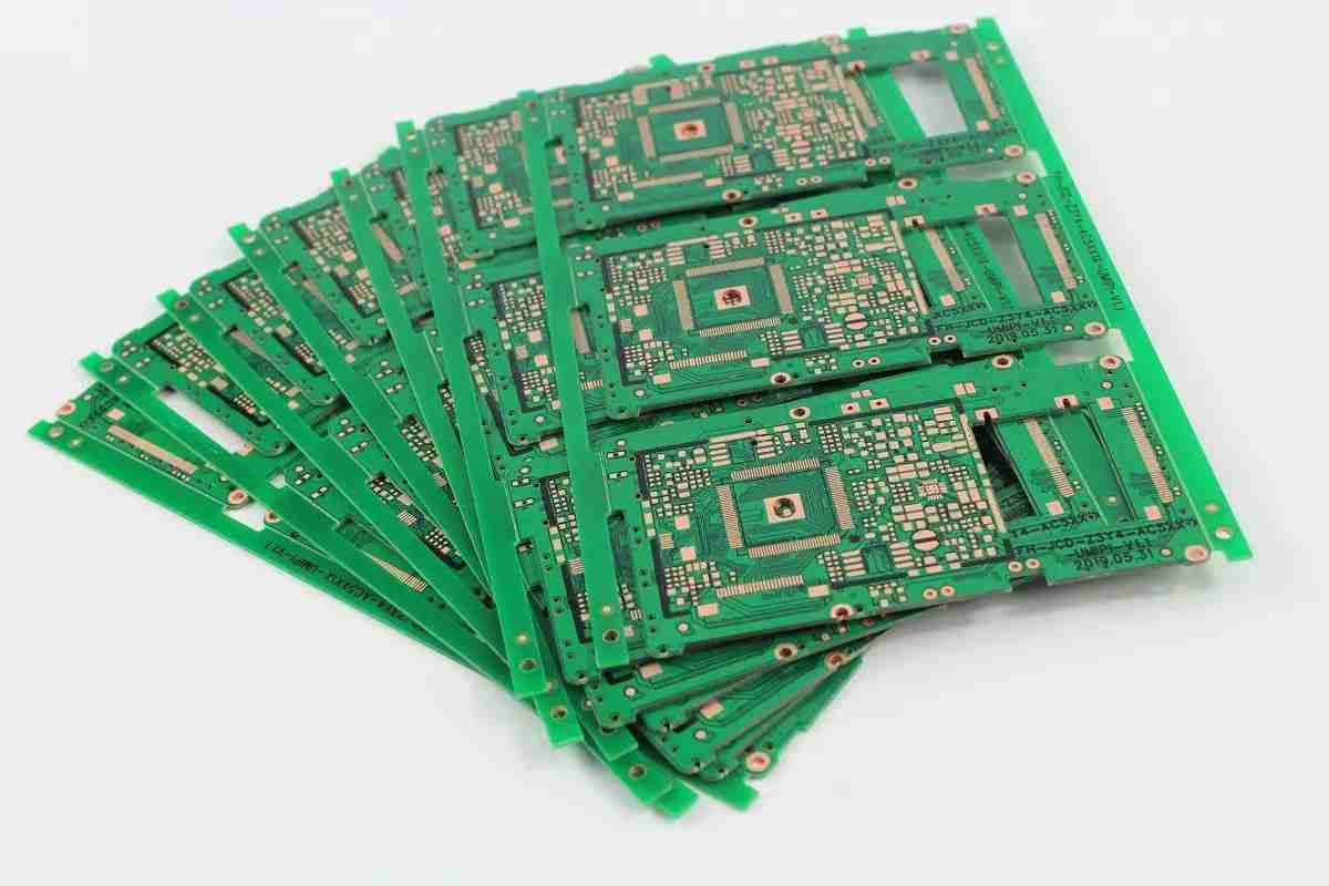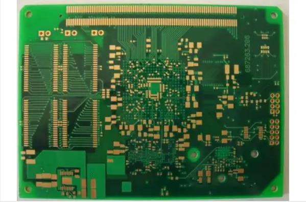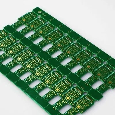
The PCB manufacturer will explain the mixed signal PCB design to you, and the key points in the design process
Mixed signal PCB design is a complex process, and the following points should be paid attention to in the design process:
(1) PCB is divided into independent analog part and digital part
(2) Appropriate component layout
(3) A/D converter placed across partitions
(4) Do not divide the ground: lay it uniformly under the analog part and digital part of the circuit board
(5) In all layers of the circuit board, digital signals can only be wired in the digital part of the circuit board; Analog signals can only be wired in the analog part of the circuit board
(6) Realize the division of analog and digital power supply
(7) The wiring shall not span the gap between the divided power planes
(8) The signal lines that must cross the gap between the split power supplies shall be located on the wiring layer adjacent to the large area
(9) Analyze the actual flow path and mode of return ground current
(10) Apply the correct routing rules

Circuit Measures in PCB Design
When designing electronic circuits, we pay more attention to the actual performance of the product than to the electromagnetic compatibility characteristics, electromagnetic interference suppression and electromagnetic anti-interference characteristics of the product. To achieve the purpose of electromagnetic compatibility, we must take necessary circuit measures, that is, add necessary additional circuits on the basis of the circuit schematic to improve the electromagnetic compatibility of the product, The following circuit measures can be adopted in actual PCB design:
(1) The method of connecting a resistance in series on the PCB wiring can reduce the jump rate of the lower edge of the control signal wire
(2) Try to provide some form of damping for relays (high-frequency capacitors, reverse diodes, etc.)
(3) The signal entering the PCB shall be filtered, and the signal from the high noise area to the low noise area shall also be filtered. At the same time, the serial terminal resistance shall be used to reduce the signal reflection
(4) The useless end of MCU shall be connected to the power supply or ground through the corresponding matching resistance
Or defined as an output terminal, the power and ground terminals on the integrated circuit should be connected, not suspended
(5) The unused gate circuit input terminal shall not be suspended, but connected to the power supply or grounding through the corresponding matching resistance. The unused op amp positive input terminal shall be grounded, and the negative input terminal shall be connected to the output terminal
(6) Set a high-frequency decoupling capacitor for each integrated circuit. Add a small high-frequency bypass capacitor to each electrolytic capacitor
(7) When using high-capacity tantalum capacitor or polyester capacitor instead of electrolytic capacitor as the charging and discharging energy storage capacitor on the circuit board, when using tubular capacitor, the circuit whose shell is to be grounded will return. The biggest difference is that in addition to the ground coupling, the differential line also has mutual coupling. The one with strong coupling becomes the main return path. In PCB circuit design, generally, the coupling between differential cabling is small, usually accounting for only 10-20% of the coupling degree, and more coupling to the ground, so the main return path of differential cabling still exists in the ground plane. When the local plane is discontinuous, the coupling between differential routing will provide the main return path in the area without reference plane. Although the discontinuity of the reference plane has no serious impact on the differential routing, it will still reduce the quality of differential signal and increase EMI, which should be avoided as far as possible.
Some designers also believe that the reference plane below the differential wiring can be removed to suppress some common mode signals in differential transmission, but this practice is not desirable in theory. How to control the impedance? Failure to provide a ground impedance loop for common mode signals will inevitably result in EMI radiation, which will do more harm than good. Circuit board assembly, circuit board design, and circuit board processing manufacturers explain the digital analog mixed signal PCB design of circuit board manufacturers.


