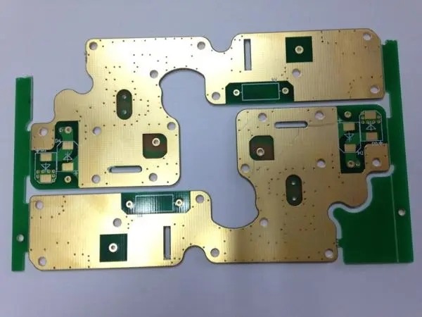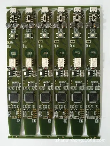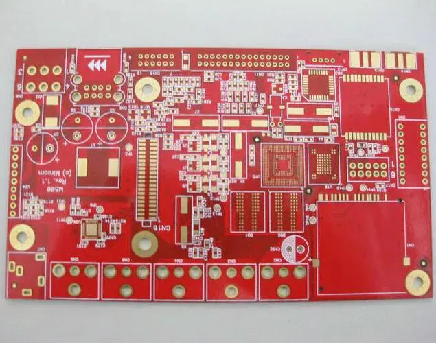
PCB assembly and PCB processing manufacturers explain the knowledge about FPC in mobile phone PCB design and PCB requirements for non electrolytic nickel coating
Why use FPC circuit board?
The main board of the mobile phone and the small board of a circuit module are electrically connected through FPC. For example, camera FPC, screen FPC, TP FPC
Audio small board FPC, etc; Generally, the PFC key mainly includes the power on key, volume key, other function keys, etc.
1) Number of layers: generally 2 layers.
2) Material selection: To ensure bending performance, it is recommended to select 0.5mil/0.5oz single-sided substrate, calendered copper (RA); Cover layer is 0.5mil.
3) Line in bending area:
a) No through hole is allowed in the part to be bent;
b) The protective copper wire shall be added at the most two sides of the line. If the space is insufficient, the protective copper wire shall be added at the inner R corner of the bending part. c) The connecting part of the line shall be designed as an arc.
4) Air gap: The bending area needs to be layered to remove the glue so as to disperse the stress. The bending area shall be as large as possible without affecting the assembly.

5) Shielding layer: At present, the shielding layer of mobile phone PCB design generally adopts silver paste and copper foil.
a) Silver paste shielding layer is used to reduce the actual number of active layers, facilitate assembly, simple process and low cost. However, the resistance of silver paste is high, about 1 ohm, because it is a mixture. Therefore, the silver paste layer cannot be directly designed as the ground wire.
b) The copper foil shielding layer has two more active layers, which increases the cost, but has low resistance. It can be directly designed as a ground wire.
c) Silver foil shielding layer, the cost is too high.
PCB requirements for non electrolytic nickel coating
The non electrolytic nickel coating shall perform several functions:
Surface of gold precipitation
The ultimate purpose of the circuit is to form a connection with high physical strength and good electrical characteristics between PCB board and components. If there is any oxide or contamination on the PCB surface, the current weak flux used for this welding connection will not occur.
Gold naturally precipitates on nickel and will not be oxidized during long-term storage. However, gold will not precipitate on oxidized nickel, so nickel must be kept pure between nickel bath and gold dissolution. In this way, the first requirement of nickel is to keep it free of oxidation for a long enough time to allow the precipitation of gold. The element has developed a chemical bath to allow 6-10% phosphorus content in nickel precipitation. This phosphorus content in the non electrolytic nickel coating is considered as a careful balance between bath control, oxides, and electrical and physical properties.
hardness
Non electrolytic nickel coatings are used in many applications requiring physical strength, such as automotive transmission bearings. The need for PCB boards is far less stringent than these applications, but for wire bonding, touch pad contact points, edge connectors, and processing sustainability, a certain hardness is important.
Lead wire bonding requires a nickel hardness. If the lead deforms the sediment, loss of friction may occur, which helps the lead "melt" into the substrate. SEM photos show no penetration into the surface of flat nickel/gold or nickel/palladium (Pd)/gold.
Electrical characteristics
Because it is easy to make, copper is chosen as the metal for circuit formation. Copper conducts electricity better than almost every metal. Gold also has good conductivity and is the perfect choice for the outermost metal, because electrons tend to flow on the surface of a conductive path ("surface" benefits). PCB assembly and PCB processing manufacturers explain the knowledge about FPC in mobile phone PCB design and PCB requirements for non electrolytic nickel coating.


