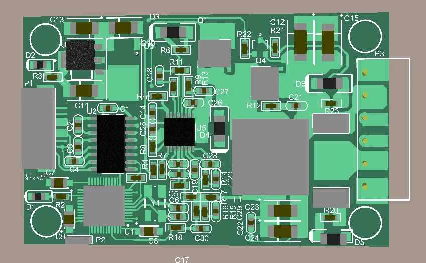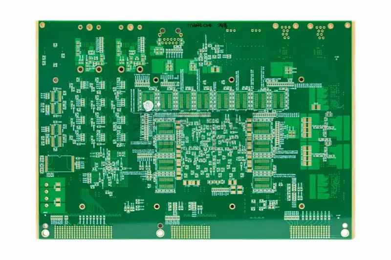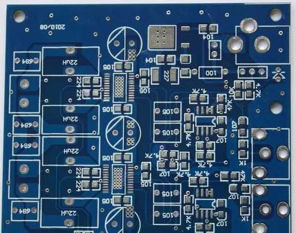
The circuit board manufacturer explains the rules for viewing elements of circuit board layout design
Circuit board design and circuit board processing manufacturer explain circuit board manufacturer explain circuit board layout design view element rules
DFM requirements for PCB layout
1 The optimal process route has been determined, and all devices have been placed on the board.
2 The coordinate origin is the intersection of the left and lower extension lines of the board frame, or the lower left pad of the lower left socket.
3 The actual size of PCB, position of locator parts, etc. are consistent with the process structure element diagram, and the layout of device PCB boards in areas with limited device height requirements meets the requirements of the structure element diagram.
4 The position of dial switch, reset device and indicator light is appropriate, and the handle bar does not interfere with its surrounding devices.
5 The smooth radian of the outer frame of the plate is 197mil, or it is designed according to the structural dimension drawing.
6 Ordinary plate has 200 mil process edge; The left and right sides of the backplane are reserved with process edges larger than 400 mils, and the upper and lower sides are reserved with process edges larger than 680 mil. The device placement does not conflict with the window opening position.
7 All kinds of additional holes (ICT positioning hole 125mil, handle bar hole, elliptical hole and optical fiber bracket hole) to be added are not omitted and set correctly.
8 The pin spacing, device direction, device spacing and device library of devices processed by wave soldering shall take into account the requirements of wave soldering processing.
9. The PCB layout spacing of devices shall meet the assembly requirements: surface mounted devices shall be more than 20mil, IC shall be more than 80mil, and BGA shall be more than 200mil.
10. The distance between the crimping parts and the components whose surface is higher than it is greater than 120mil, and there is no component in the through area of the crimping parts on the welding surface.
11 There are no short devices between high devices, and no patch devices and short and small plug-in devices are placed within 5 mm between devices with a height greater than 10 mm.
12 Polarity devices are marked with polarity silk screen. The X and Y directions of the same type of polar plug-in components are the same.
13 All components are clearly marked, without P *, REF and other unclear marks.
14 The surface containing the patch device has three positioning cursors, which are placed in an "L" shape. The distance between the positioning cursor center and the plate edge is greater than 240mil.
15 If it is necessary to do panel splicing, PCB layout shall be convenient for panel splicing, PCB processing and assembly.
16 The notched plate edges (irregular edges) shall be supplemented by milling grooves and stamp holes. The stamp hole is non-metallic hollow, with a diameter of 40 mil and a margin of 16 mil.

17 The test points used for debugging have been added in the schematic diagram, and the position in the PCB layout is appropriate.
Thermal design requirements for PCB layout
18 The heating elements and the exposed components of the shell shall not be close to the wires and thermal sensors, and other components shall also be properly away.
19 The radiator is placed in consideration of convection. There is no interference of high components in the projection area of the radiator, and the range is marked on the installation surface with a silk screen.
20 The PCB layout considers that the heat dissipation channel is reasonable and smooth.
21 The electrolytic capacitor shall be properly away from the high heat device.
The heat dissipation of high-power devices and devices under the daughter board is considered.
Signal integrity requirements for PCB layout
23 The starting end matches the device close to the sending end, and the terminal matches the device close to the receiving end.
24 Decoupling capacitors placed close to related devices
25 Crystals, crystal oscillators, clock drive chips, etc. are placed close to related devices.
26 High speed and low speed, digital and analog PCB layout is separated by module.
27 Determine the bus topology according to the analysis and simulation results or existing experience to ensure that the system requirements are met.
28 If the board is changed, simulate the signal integrity problems reflected in the test report and provide solutions.
29 PCB layout of synchronous clock bus system meets timing requirements.
EMC Requirements
Inductors, relays, transformers and other inductive devices prone to magnetic field coupling shall not be placed close to each other. When there are multiple inductance coils, the direction is vertical and uncoupled.
31 In order to avoid electromagnetic interference between components on the welding surface of a single board and adjacent boards, no sensitive devices or strong radiation devices are placed on the welding surface of a single board.
32 The interface devices are placed close to the board edge, and appropriate EMC protection measures have been taken (such as measures with shielding shell, power supply ground hollowing, etc.) to improve the EMC capability of the design.
33 The protection circuit is placed near the interface circuit, following the principle of protection before filtering.
34 Devices with high transmission power or special sensitivity (such as crystal oscillator, crystal, etc.) are more than 500mil away from the shield and shield housing.
35 A 0.1uF capacitor is placed near the reset line of the reset switch, and the reset device and reset signal are far away from other strong components and signals.
Layer setting and power ground separation requirements
37 When two signal layers are directly adjacent, vertical wiring rules must be defined.
38 The main power layer shall be adjacent to its corresponding stratum as much as possible, and the power layer shall meet the 20H rule.
39 Each wiring layer has a complete reference plane.
40 Multilayer boards are laminated and core materials (CORE) are symmetrical to prevent uneven distribution of copper sheet density and asymmetric medium thickness from warping.
41 The plate thickness shall not exceed 4.5mm. For the plate thickness greater than 2.5mm (the back plate greater than 3mm), the process personnel shall confirm that there is no problem in PCB processing, assembly and equipment, and the PC card thickness is 1.6mm.
42 If the thickness diameter ratio of via is greater than 10:1, it shall be confirmed by the PCB manufacturer.
43 The power and ground of the optical module are separated from other power and ground to reduce interference.
44 The power and ground treatment of key components meet the requirements.
45 When impedance control is required, layer setting parameters meet the requirements.
Power module requirements
46 The PCB layout of the power supply part ensures that the input and output lines are smooth and do not cross.
When the board supplies power to the daughter board, the corresponding filter circuit is placed nearby at the power outlet of the board and the power inlet of the daughter board.
Other requirements
48 The PCB layout takes into account the smoothness of the overall routing, and the main data flow is reasonable.
49 Adjust pin assignment of devices such as drain, FPGA, EPLD and bus driver according to PCB layout results to optimize wiring.
50 For PCB layout, it is considered to appropriately increase the space at the dense wiring to avoid the situation that cannot be routed.
If special materials, special components (such as 0.5mmBGA) and special processes are adopted, the arrival date and processability have been fully considered and confirmed by PCB manufacturers and technologists.
52 The pin correspondence of the gusset plate connector has been confirmed to prevent the wrong direction and orientation of the gusset plate connector.
53 If there are ICT test requirements, the PCB layout should consider the feasibility of adding ICT test points to avoid the difficulty of adding test points in the wiring stage.
54 When high-speed optical modules are included, the optical port transceiver circuit is preferred for PCB layout.
After the completion of PCB layout, 1:1 assembly drawing has been provided for the project personnel to check whether the device packaging selection is correct against the device entity.
56 At the window opening, the inner plane has been considered to be retracted, and a suitable no wiring area has been set. The circuit board assembly, circuit board design, and circuit board processing manufacturers explain the rules of circuit board layout design inspection elements.


